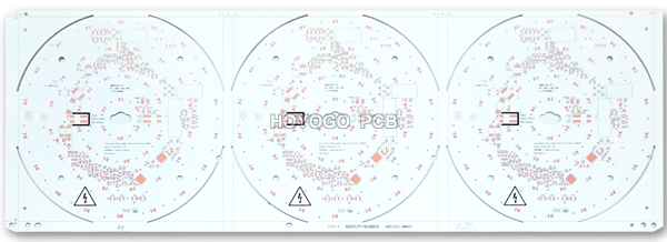
Copper clad is an important part of PCB design. The so-called copper clad is to use the unused space on the PCB as the reference surface, and then fill it with solid copper. These copper areas are also called copper pour. The significance lies in: reducing the ground wire impedance, improving the anti-interference ability; reducing the pressure and improving the power supply efficiency; connecting with the ground wire can also reduce the loop area. At the same time, it also makes the PCB not be deformed as much as possible.

At high frequencies, the distributed capacitance of the layout on the PCB will work. When the length is greater than 1/20 of the corresponding wavelength of the noise frequency, an antenna effect will occur and the noise will be emitted through the wiring.If the copper cladding in the PCB is poorly grounded, the copper cladding becomes a tool for propagating noise.Therefore, the copper cladding must be properly treated.
There are two ways to fill the PCB with grounded copper: Large area copper cladding and grid copper cladding. Large area copper cladding has the dual function of increasing current and shielding, but when wave soldering is over, the board may be lifted or even foamed. Therefore, a large area of copper cladding will also open several slots to reduce the foaming of copper foil. From the perspective of heat dissipation, grid copper is more beneficial.It reduces the heated surface of the copper and acts as an electromagnetic shield. But the grid consists of routes in the staggered direction. For a circuit, the width of the route is its corresponding electrical length. When the working frequency is not very high, the role of the grid lines is not obvious. However, once the electrical length matches the operating frequency, the circuit becomes inoperable and transmits signals that interfere with the operation of the system. Therefore, for the copper clad method, it is necessary to select according to the actual working conditions of the PCB.
PCB Copper Clad Notes:
1.For single point connections to different locations, the method is to connect through resistors, beads or inductors.
2.The crystal oscillator in the circuit is a high frequency emission source. It grounds the crystal oscillator separately after encircling the copper cladding of the crystal oscillator.
3.Regarding dead zone problem, if you think it is big, then define a ground hole to add it.
4.When starting the layout, the ground wire should be well grounded. It is not possible to rely on the adding vias to eliminate the ground pins that are connected after copper clad. This effect is very poor.
5.It is best not to have sharp corners on the board. Because from an electromagnetic point of view, this constitutes a transmitting antenna, which always has an effect on it, so it is recommended to use the edge of the arc.
6.The layout area of the middle layer of the multi-layer board does not need copper clad. Because it is difficult for people to make this copper cladding "good grounding".
7.The metal inside the equipment must be “well grounded”.
8.The heat-dissipating metal block of the three-terminal regulator and the grounding isolation zone near the crystal oscillator must be well grounded.