3-step HDI PCB | HYG603R12007A
Product Image
Product Details
Special Request:
1. 3-step HDI PCB.
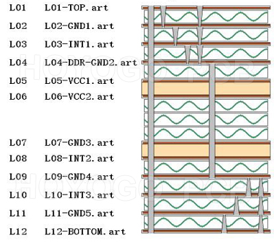
2. The blind vias are located between layers L1-L2, L2-L3,
L3-L4, L9-L10, L10-L11, and L11-L12, as well as L9-L12.
They are laser-drilled and require copper filling and capping.
3. 18 groups of Impedance Control.
4. BGA PAD: 0.25mm.
Layer: 12L
Base Material: FR4 TG≥170℃
Board Thickness: 1.5mm
Outer Layer Final Copper Thickness: 30um
Inner Layer Final Copper Thickness: 1/3OZ+plating
Surface Finished: ENIG
Unit Size(mm): 191.00*123.00
Min. W/S(mil): 1.8/2.9
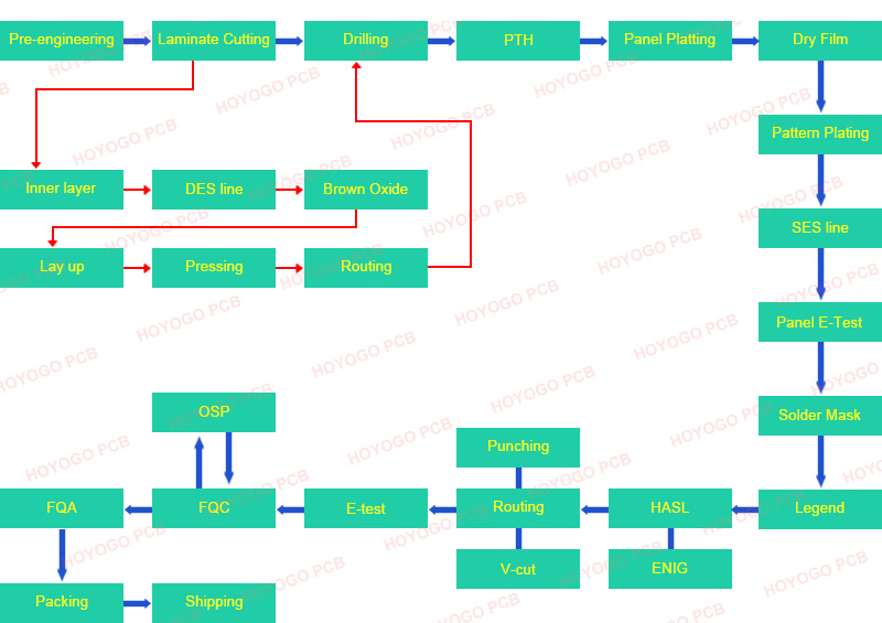
Min. Hole Size: 0.125mm Production Process
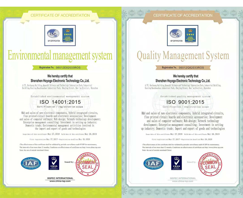
ISO Certification
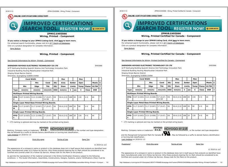
UL Certification
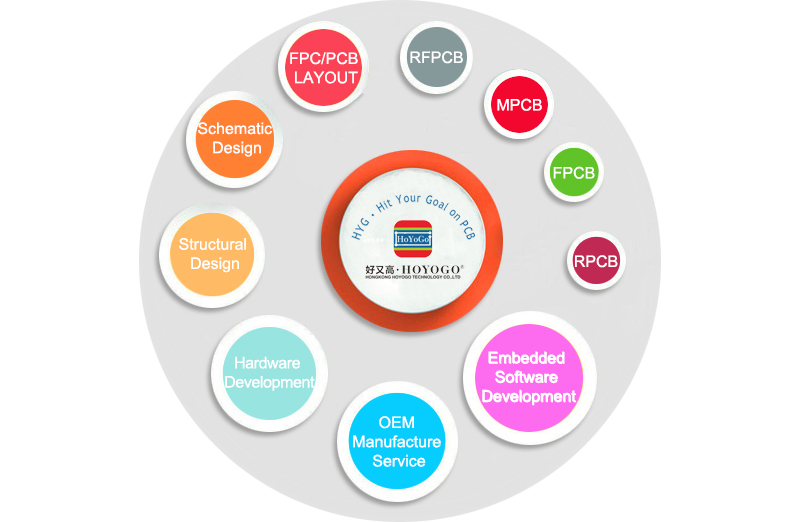
Application areas

Who will be our parters
FAQ
-
What’s kind of PCB can you produce?
-
Our production is producing rigid PCB from 2~56layer with small- medium- mass volume. In the meantime, we can offer you FPC, Rigid-flex, HDI, all other special PCBs from our partner production.
Contact us
Welcome to the HOYOGO website!
HONGKONG HOYOGO TECHNOLOGY CO.,LTD
SHENZHEN HOYOGO ELECTRONIC TECHNOLOGY CO.,LTD
Tel : (+86)-755-2300 1582
Fax : (+86)-755-2720 6126
Email : sales@hygpcb.com
Add: 8F, Second-A Building, Daji Hui Innovation Industrial Center, Shajing Street Bao'an District, Shenzhen. 518104/ P.R.C.


 English
 Français
 Deutsch
 Português
 Pусский
 中文
中文