HYG089R04371A
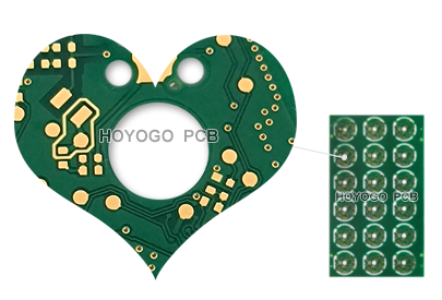
Product Image
Product Details
1-step HDI Blind & Buried Via PCB
Special Request:
1. Buried vias between L2 and L3;
2. HDI blind vias between L1–L2 and L4–L3, resin-filled and copper-capped;
3. Impedance control required.
Layer: 4L
Base Material: FR4, IT150GTC, PP IT-150GBS
Board Thickness: 0.5+/-0.1mm
Outer Layer Final Copper Thickness: 30UM
Inner Layer Final Copper Thickness: 25UM
Surface Finished: ENIG
Unit Size(mm): 28.64*30.40
Min. W/S(mil): 3.93/3.93
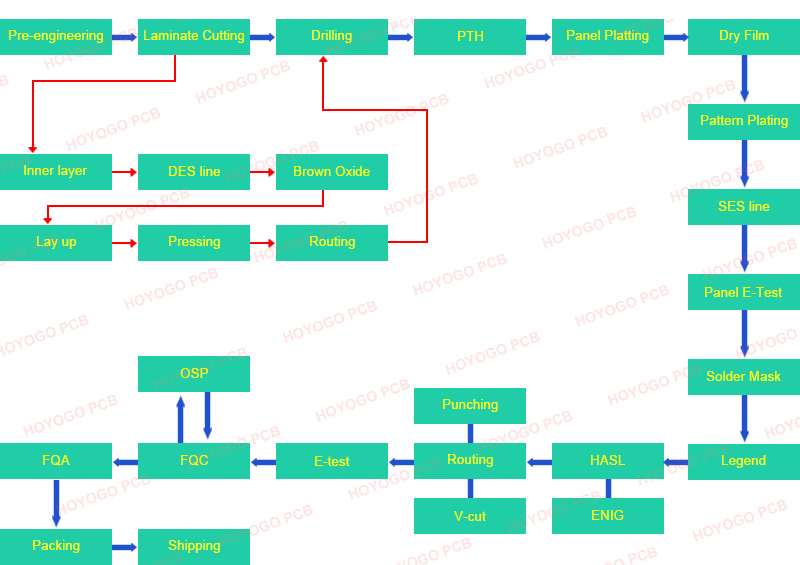
Min. Hole Size: 0.1mm Production Process
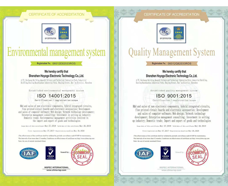
ISO Certification
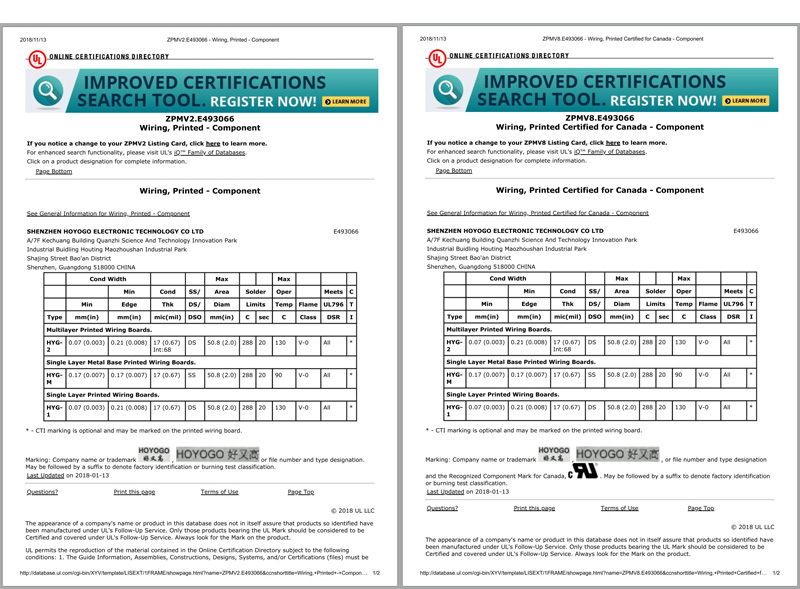
UL Certification
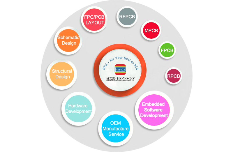
Application areas

Who will be our parters
FAQ
-
What’s your quality standard? What’s certificates do you have?
-
Our production is strictly following high quality system of automotive products, we certified with ISO9001, ISO14001, ISO13485 and IATF16949 and C-UL-S. All products strictly follow acceptance standard IPC-A-600-H and IPC-6012.
Contact us
Welcome to the HOYOGO website!
HONGKONG HOYOGO TECHNOLOGY CO.,LTD
SHENZHEN HOYOGO ELECTRONIC TECHNOLOGY CO.,LTD
Tel : (+86)-755-2300 1582
Fax : (+86)-755-2720 6126
Email : sales@hygpcb.com
Add: 8F, Second-A Building, Daji Hui Innovation Industrial Center, Shajing Street Bao'an District, Shenzhen. 518104/ P.R.C.


 English
 Français
 Deutsch
 Português
 Pусский
 中文
中文