Welcome to visit Hoyogo website, let's connect the world together!
Customer service hotline:+86 13723413985 or 400 058 2288
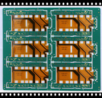
|
Layer:2 |
Base Material:FR4 |
|
Board Thickness:0.8mm |
Unit Size:52.06x160.85 |
|
W/S:8/8.7 |
Copper OZ:1OZ |
|
Surface Finish:HASL Lead Free |
Solder Mask:Green |
Products List
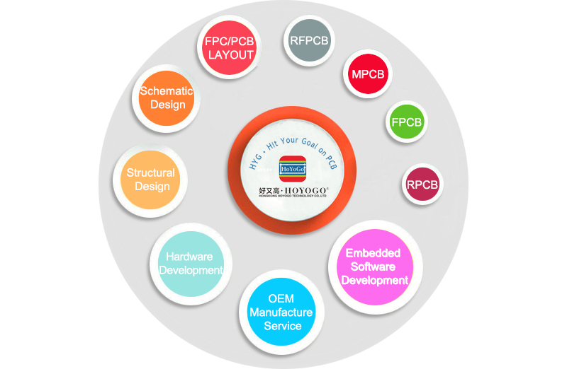
HOYOGO can support all your pcb requirements from simple single sided conventional FR4 pcbs to complex exotic HDI requirements and PCB assembly.
Conventional FR4 1 to 56 layer
High TG and or heavy copper
High frequency exotic substrate
HDI
Gold finger
Hard gold plating
Flexible pcb
Rigid‐Flex pcb
IMS pcb (Aluminum, copper base/core)
Medical requirements ‐ ISO13485 certified suppliers
Automotive requirements – TS16949 certified suppliers
Standard and quick turn to 3 days available
|
|
|
|
|
|
|
|
PCB components
Printed circuit boards are mainly composed of pads, vias, mounting holes, wires, components, connectors, fillers, electrical boundaries, etc. The main functions of each component are as follows:
1.Pads: Metal holes used to solder component pins.
2.Via: Metal hole used to connect component pins between layers.
3.Mounting hole: Used to fix the printed circuit board.
4.Conductor: An electrical network copper film used to connect component pins.
5.Connectors: Components used to connect between circuit boards.
6.Fill: The copper used for the ground network can effectively reduce the impedance.
7.Electrical Boundary: Used to determine the size of the circuit board. Components on all circuit boards must not exceed this boundary.

|

|

|

|
We are winning our customer with our good quality, our comprehensive full service and our competitive price, and I am hoping to provide you with our best services too!
Any question or RFQ, please E-mail to me, I will be pleased and do reply you within 2 hours.
Welcome to the HOYOGO website!
HONGKONG HOYOGO TECHNOLOGY CO.,LTD
SHENZHEN HOYOGO ELECTRONIC TECHNOLOGY CO.,LTD
Tel : (+86)-755-2300 1582
Fax : (+86)-755-2720 6126
Email : sales@hygpcb.com
Add: 8F, Second-A Building, Daji Hui Innovation Industrial Center, Shajing Street Bao'an District, Shenzhen. 518104/ P.R.C.


 English
 Français
 Deutsch
 Português
 Pусский
 中文
中文


