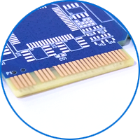
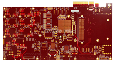
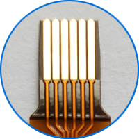
On the computer memory bank and the graphics card, we can see a row of golden conductive contacts, the surface of which is gold-plated and the conductive contacts are arranged like fingers, so it is called "gold finger". All signals are transmitted through it. It is also known as Edge Connector in the PCB design. Next, let's learn the surface treatment and processing details of the gold finger PCB.

The surface treatment of the gold finger PCB is as follows:
1. Plating Gold/ENEG:
Its thickness can reach 3-50u". Due to its superior electrical conductivity, oxidation resistance and wear resistance, it is widely used in gold finger PCB that require frequent insertion and removal, or on PCB boards that require frequent mechanical friction. However, because the cost of gold plating is extremely high, it is only applied to local gold plating such as gold fingers.

2. Immersion Gold/ENIG:
The conventional thickness is 1u", up to 3u". The immersion gold surface treatment has excellent conductivity and solderability, and has good flatness. Therefore, it is widely used in high-precision PCB boards with bonded IC and other designs such as BGA. For the gold finger PCB with low wear resistance requirements, the whole plate immersion gold process can also be selected. The cost of the immersion gold process is much lower than that of the plating gold process. The color of the immersion gold process is golden.

Gold finger processing details in PCB:
1) In order to increase the wear resistance of the gold finger, the gold finger usually needs to be plated with hard gold;
2) Gold fingers need to be chamfered, usually 45°, other angles such as 20°, 30°, etc; If there is no chamfer in the design, there is a problem;
3) The immersion tin and the immersion silver pad need a minimum distance of 14 mil from the tip of the gold finger; It is recommended to design the pad distance from the gold finger and the via pad to 1mm or more;
4) Gold finger needs to do a whole piece of solder mask opening treatment
5) Do not pour copper on the surface of the gold finger;
6) All layers of the inner layer in the gold finger need to be cut by copper, usually the width of the copper is 3mm;
Hard gold Soft gold:
Hard gold, generally a harder gold compound. Soft gold, generally a softer gold.
The gold finger plays the role of transmitting signals, so it must have good electrical conductivity, wear resistance, oxidation resistance and corrosion resistance. Pure gold texture is relatively soft, so gold fingers generally do not use pure gold, but only plate a layer of "hard gold (gold compound)"
So has the PCB used “soft gold”? The answer is certainly yes. For example, the contact surface of some mobile phone keys, the aluminum wire on the COB, and the like. Nickel gold is deposited on the PCB using soft gold plating, which is more flexible in thickness control.
Tip: Regardless of whether the PCB is plated with soft gold or hard gold, the gold content will not be too much.You should not dismantle electronic devices to get gold.