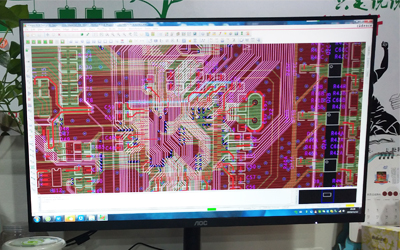
A multi-layer PCB consists of connecting wires on several insulating substrates and pads for assembling soldered electronic components. Multi-layer PCB not only helps the machine to conduct various different circuits, but also is insulated and does not allow electricity and electricity to collide with each other, so it is absolutely safe. If you want a PCB with good performance, you have to design it carefully.

1. Board Shape, Size and Number of Layers
Shape & Size: We need to consider the overall structure of the product, production process and so on. In order to facilitate assembly, improve production efficiency, and reduce labor costs, the shape and size of the PCB should be as simple as possible, and usually a rectangle having no large difference in aspect ratio.
Layer: It depends on circuit performance requirements, board size and circuit density.
Every layer should be symmetrical, especially copper layers, such as four, six, eight layers, and the like. If the lamination is not symmetrical, it tends to cause warpage on the surface of the board. Surface mounted multi-layer boards should attract more attention.
2. Components Location and Placement Direction
The position and orientation of components should be in line with the circuit principle. If the location of the components is not properly placed, the performance of the PCB will be affected. The requirements for high frequency analog circuits are clearly more stringent. At the beginning, you need to analyze the circuit principle in detail, then confirm the location of the special components and arrange the other components.
3. Wiring Layer & Wiring Area
Outer Layer Wiring: The solder side requires more wiring, and the component side requires less wiring, which is facilities PCB maintenance and troubleshooting.
Inner Layer Wiring: It is usually a thin, dense wire and a signal line that is susceptible to interference. Large areas of copper foil should be evenly distributed throughout the inner and outer layers, which helps to reduce PCB warpage and achieve a more uniform coating on the surface during the plating process.
The conductive pattern of the inner and outer layer wiring areas should be more than 50 mils from the edge of the PCB to prevent subsequent shape processing from the printed wiring an causing interlamination short circuits.
4. Drill size & PAD
They are related to the component size of the component selected. If the drilling is too small, it will affect the insertion and tinning of the device; if the drilling is too large, the solder joint will be insufficient during the SMT process.
For high-density multi-layer PCBs, the via hole diameter should normally be controlled within the range of board thickness: aperture ≤ 5:1.
5. Wire Orientation & Line Width
The lines of two adjacent PCBs should be as perpendicular to each other or diagonal lines, curves to reduce the interlayer coupling and interference of the substrate. And the wire should be as short as possible, especially for small signal circuits, the line is short, the resistance is small, and the interference is small.
When wiring, the width of the lines should be as uniform as possible, which is good for impedance matching.
6. Power Plane & Ground Plane Division
The multi-layer PCB has at least one power plane and one ground plane. The second layer is ground plane for shielding devices, and all signal layers have reference planes. The formation should not be adjacent to the signal layer. If the ground plane is adjacent to the signal layers, the signal direction should be arranged in the vertical direction, and the key signal reference plane should be the complete ground plane without crossing the partition. Since all voltages on the PCB are connected to the same power plane, the power plane must be partitioned. The size of the partition line is generally 20 to 80 mils. The higher the voltage, thicker partition line.
7. Safety Clearance
The safety clearance should be set to meet the electrical safety requirements. When the clearance can be arranged under the wiring, large values should be taken as much as possible to improve the yield during PCB making and reduce the hidden troubles of the finished PCB.
8. Improve the Anti-jamming Capability of the Whole PCB
The design of multi-layer PCB must also pay attention to the anti-interference ability of the whole board. The general methods are as follows:
A. Add filtering capacitance near the power supply and ground of each IC. The capacity is generally 473 or 104.
B. For sensitive signals on the PCB, the accompanying shielded lines should be added separately, and there should be as little wiring as possible near the signal source.
C. Choose a reasonable grounding point.