Welcome to visit Hoyogo website, let's connect the world together!
Customer service hotline:+86 13723413985 or 400 058 2288
|
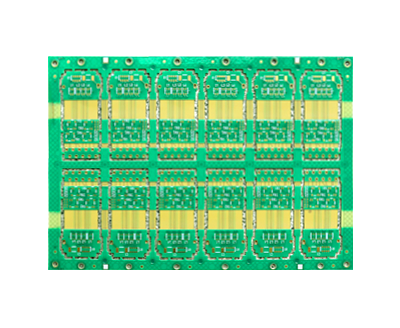
Layer:4 |
Base Material:FR4+PI |
|
Board Thickness:0.60mm |
Unit size:119.02 x 84.30mm |
|
W/S(mil):3u |
Surface Finishing: ENIG Thickness |
|
Solder Mask:Green |
Copper OZ: 2OZ |

|
Plant invested capital |
92 mil USD |
|
Address |
Mass production---Qingyuan |
|
Quick-turn production---shenzhen |
|
|
Monthly |
350,000 sqm |
|
Staff |
5000 |
|
Sales Revenue 2017 |
50 mil USD |
|
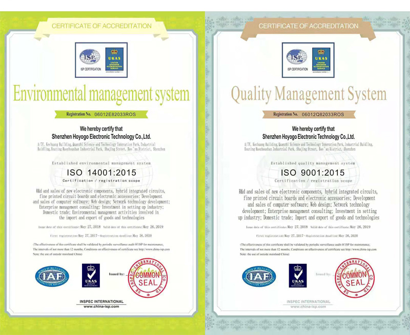
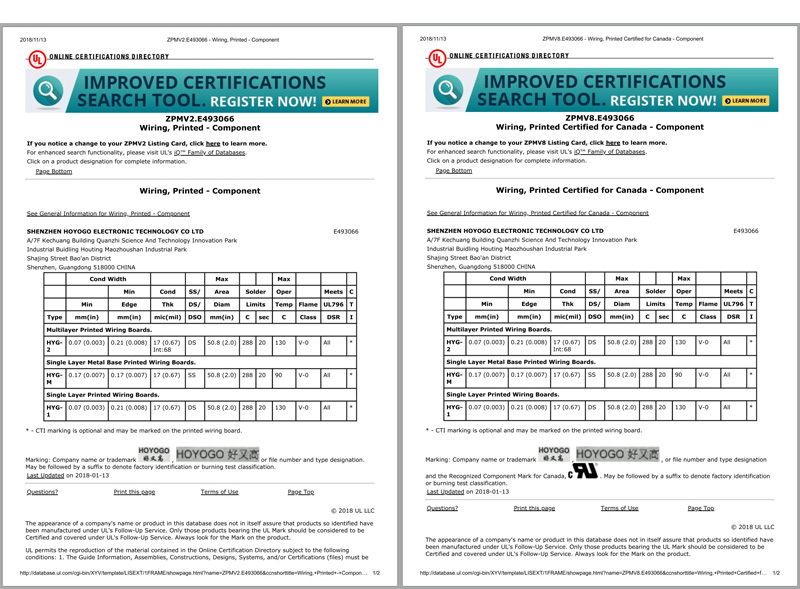
Quality system |
C-UL-US, ISO9001, ISO/TS16949 |
|
|
|

Features: FPC must have MARK mark for substrate positioning, FPC itself should be flat. FPC is difficult to fix, consistency is difficult to guarantee when mass production, high equipment requirements. In addition, the control of solder paste and placement process is more difficult.
The key process: 1.FPC soft board fixing: It is fixed on the pallet from the printing patch to reflow soldering. The used pallet requires a small thermal expansion coefficient.
The placement accuracy is more than 0.65mm for the QFP lead spacing: the pallet is placed on the positioning template. The FPC is fixed on the pallet with a thin high-temperature tape, and then the pallet is separated from the positioning template for printing. The high temperature adhesive tape should have a moderate viscosity. After reflow soldering must be easy to peel, and there is no residual glue on the FPC.
The placement accuracy is less than 0.65mm for QFP lead spacing: The pallets are customized, and their process requirements must be minimally deformed after multiple thermal shocks. There is a T-shaped positioning pin on the pallet. The height of the pin is slightly higher than that of the FPC.

1 Material selection [1]
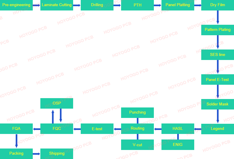
2 production process and control of key parts
2.1 production process
2.2 Graphical transfer of inner monolithic
2.3 Multi-layer positioning of flexible materials
2.4 Lamination
2.5 Drilling
2.6 Drilling and Erosion
2.7 electroless copper plating, copper plating
2.8 Surface Solder Mask and Solderability Protective Layer
2.9 Shape Processing

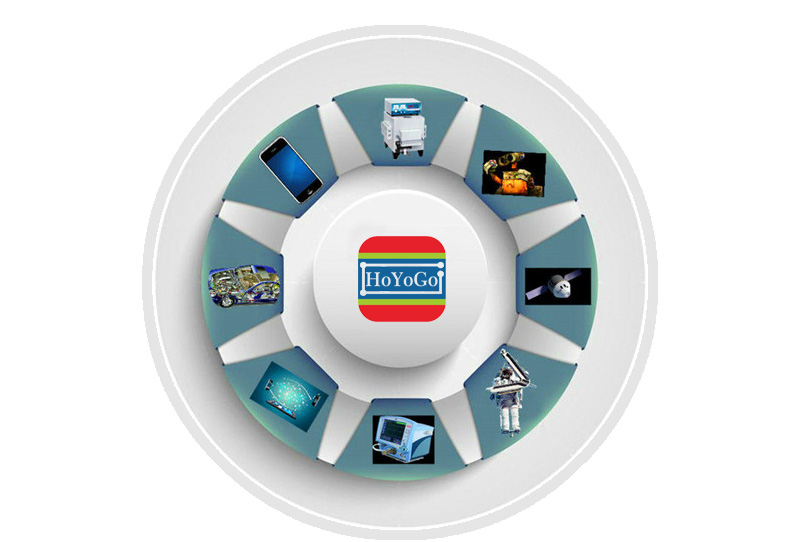
The characteristics of FPC determine its application area to cover all the application fields of the FPC in the PCB, such as:
mobile phone
Key board and side keys
Computer and LCD screen
Motherboard and display, etc.
CD Walkman
Drive
NOTEBOOK.
Components such as a suspension circuit (HD) of a hard disk drive and an xe package board.

|

|
 |
Welcome to the HOYOGO website!
HONGKONG HOYOGO TECHNOLOGY CO.,LTD
SHENZHEN HOYOGO ELECTRONIC TECHNOLOGY CO.,LTD
Tel : (+86)-755-2300 1582
Fax : (+86)-755-2720 6126
Email : sales@hygpcb.com
Add: 7A Quanzhi Science and Technology Innovation Park,Shajing Street, Bao'an District, Shenzhen. 518104/ P.R.C.


 English
 Français
 Deutsch
 Português
 Pусский
 中文
中文

