Welcome to visit Hoyogo website, let's connect the world together!
Customer service hotline:+86 13723413985 or 400 058 2288
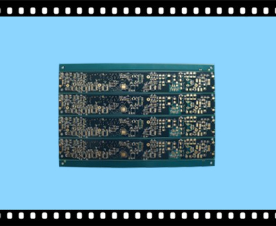
|
Layer: 6 |
Base Material: FR4 IT-158 |
|
Board Thickness:1.574mm |
Unit size: 29.000 x 197.000mm |
|
w/s(mil): 6/6 |
Surface Finishing:ENIG Thickness |
|
Solder Mask: blue |
Copper OZ:1OZ |
|
Total Holes:371 |
Silkscreen: While |
1.Field of application
Multi-layer PCBs are mainly used for professional electronic equipment, computers and military equipment, especially in the case of weight and volume overload. Multi-layer PCBs are also very useful in high-speed circuits. Multilayer PCBs provide more space for conductor patterns and power supplies
A multi-layer PCB consists of two or more PCBs with reliable pre-defined interconnections stacked on top of each other. In a multi-layer PCB, there are at least three conductive layers, two of which are on the outside and one layer is synthesized on an insulating board. Due to the complex manufacturing process and lower production costs, the cost of multilayer PCBs is relatively high.
The emergence of multi-layer PCBs stems from the development of high-speed, multi-functional, large-capacity, and small-size electronic technologies. On the one hand, as electronic devices have become smaller and smaller, due to the space available, single-sided PCBs and double-sided printed PCBs cannot match increased packing density. On the other hand, there are many problems in the PCB layout such as noise, stray capacitance, crosstalk and so on. Therefore, the design of the PCB must aim to minimize the length of the signal lines and avoid parallel routing. Obviously, a single-sided or double-sided PCB cannot meet the requirements because of the limited number of intersections that can be achieved. With a large number of interconnects and crossover requirements, the PCB can achieve satisfactory performance unless the PCB is extended to more than two layers. Multilayer PCB is listed. With the help of state-of-the-art PCB manufacturing equipment and the latest inspection equipment, CSL can produce up to 24 layers of close-packed multilayer PCBs.
At present, multi-layer PCBs have been widely used in various electronic devices. Because of their high packing density, small size, and good quality, they have become an important component of electronic components. Reliability, flexibility, and impedance of the circuit structure; Form high-s

|

|

|
2.PCB industry chain
| Upstream raw materials | Midstream Manufacturing |
Downstream applications |
||||
|
|
|
|
|
|
|
|
|
|
|
|
|
|
|
|
|
|
|
|
|
|
|
|
|
|
|
|
|
|
|
|
|
|
|
|||||
|
|
|
|
|
|||
|
|
|
|
|
|||
2.1 Upstream: (raw materials)
The main raw material cost of PCB comes from the CCL. The main cost of CCL comes from copper foil, fiberglass cloth, resin and other manufacturing expenses (including labor, storage and logistics, equipment depreciation, water and electricity coal, etc.), among which the top three raw materials The proportion is 3/4, and its price is a key factor affecting the cost of CCL.
Copper foil is the raw material with the largest proportion of the cost of CCL, which is about 30% (thick) and 50% (thin). The price increase of copper foil is the main driving force for price increase of CCL.


2.2 Midstream (Manufacturing)
Copper Clad Laminat (CCL), also known as copper-clad laminate, is made of reinforcing materials such as electronic grade glass fiber cloth or wood pulp paper. It is impregnated with resin and dried. The semi-cured bond sheet is coated with a thin copper foil on a single-sided, double-sided or multi-layered board surface, and is made under a special hot-pressing process condition, which is a direct raw material for the PCB and is used in many applications. Laminate production, also called core board
2.3 Downstream applications
PCBs are widely used in the computer, communications, consumer electronics, industrial control medical, military, semiconductor and automotive industries, including almost all electronic information products. Among them, computer, communication and consumer electronics are the three main application areas, occupying about 70% of the PCB industry output value.

Welcome to the HOYOGO website!
HONGKONG HOYOGO TECHNOLOGY CO.,LTD
SHENZHEN HOYOGO ELECTRONIC TECHNOLOGY CO.,LTD
Tel : (+86)-755-2300 1582
Fax : (+86)-755-2720 6126
Email : sales@hygpcb.com
Add: 8F, Second-A Building, Daji Hui Innovation Industrial Center, Shajing Street Bao'an District, Shenzhen. 518104/ P.R.C.


 English
 Français
 Deutsch
 Português
 Pусский
 中文
中文


