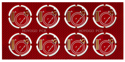
Recently,emerging HDI has attracted much attention and has become the “darling” in the PCB industry. HDI(High Density Interconnector) usually refers to a kind of PCB with high line distribution density, on which the micro-blind buried via technology is applied on the 0.1mm min hole. Because of its fast signal transmission speed, small size and cost-saving feature, it is much popular in the market, and mainly used in the high-end products such as smart phones, tablet computers and GPS navigation.
Such boards require high technical content, precise accuracy, complicated processes. It takes a long time to complete the production, and its requirements for production equipment are much higher than ordinary multi-layer boards.
The following is a type of HDI boards produced recently.

Specification:
Layer : 6L
Base Material : FR4
Board Thickness : 0.8mm
Final Copper Thickness : 1OZ
Surface Finished : ENIG
Unit Size(mm) : 24.71*24.71
Min Hole Size : 0.1mm
Min Hole Copper Thickness : 20um
Min W/S(mil) : 4.7/4.3
Solder Mark : Glossy Red
Special Request: Blind&Buried Via
Via Plug with Resin&Electroplating Flattened
This 2step HDI PCB is with multilayer arbitrary interconnection technology, specifically referring to the electrical interconnection between adjacent two or more layers through blind holes. It mainly adopts the process for via plug with resign&electroplating flattened, to make the product highly reliable and well conducted, which perfectly meets the customer's quality requirements.