Welcome to visit Hoyogo website, let's connect the world together!
Customer service hotline:+86 13723413985 or 400 058 2288
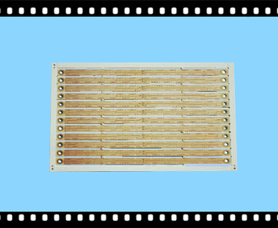
Layer:2
Base Materia:FR4 CTI175
Board Thickness:0.3mm
Unit Size:10x218mm
W/S:11.8/7.9
Copper OZ:52.9um
Surface Finishing:ENIG Thickness
Solder Mask:White
Our company can offer a massive order with cost reduction for 15%, a discount ensuring quality assurance for following reasons.
1.We are specialized in manufacturing PCB 1-28 layers, Flex-PCB, R-Flexible PCB, Aluminum PCB, HDI PCB for large volume
2.Our factory lies in Qingyuan, a northern city of Guangdong, the low-cost of labor, water & electronic power can save much production cost.
3.Our own factory land with plant floor 45,000 sqm & staff dormitory construction by ourselves saves the rent cost as well.
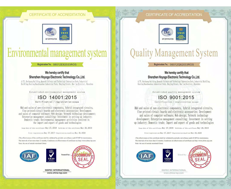
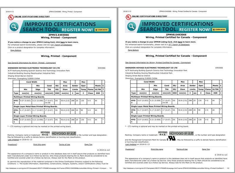
4.Certifications: C-UL-US, ISO9001, ISO/TS16949, ISO14001 Certified
5.We can reduce your PCB cost at least 30%, because we have our own large plant.

|

|

|
1. The insulation layer between two copper foils or conductor layers should be at least two sheets of film, and the thickness after pressing should not be less than 3.5 mils to prevent the copper foil from directly pressing on the glass cloth to form too high dielectric constant. Lead to poor insulation and poor adhesion.
2. In order to enable the glue to fill the voids in the board, and not to cause excessive slippage or excessive expansion of the Z direction afterwards, the original thickness of the film should be at least twice as thick as the copper. Row. The outermost layer and the outermost layer must have at least 5mil to ensure good insulation.
3. The latitude and longitude directions of the thin substrate and the film cannot be mis-mixed. The warp and weft direction of the film must be correct. The number of sheets must be symmetrically up and down to balance the resulting stress.
4. Combination method: The inner layer and the film above the six layers are fixed by rivets to prevent the pressure from being pressed together. The length and depth of the rivets are required here, and the tightness of the rivets should be noted.

|

|

|

|
Welcome to the HOYOGO website!
HONGKONG HOYOGO TECHNOLOGY CO.,LTD
SHENZHEN HOYOGO ELECTRONIC TECHNOLOGY CO.,LTD
Tel : (+86)-755-2300 1582
Fax : (+86)-755-2720 6126
Email : sales@hygpcb.com
Add: 8F, Second-A Building, Daji Hui Innovation Industrial Center, Shajing Street Bao'an District, Shenzhen. 518104/ P.R.C.


 English
 Français
 Deutsch
 Português
 Pусский
 中文
中文