Welcome to visit Hoyogo website, let's connect the world together!
Customer service hotline:+86 13723413985 or 400 058 2288
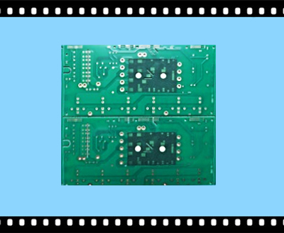
[Product details]

|

|

|

|
| Layer: 4 | Base Material: FR4 TG>=150 TD>=320 |
| Board thickness: 1.6mm | Unit Size(mm): 119 x 247 |
| Min hole size: 0.6mm | Panel Size(mm): 257 x 240 |
| Total hole: 1017/SET | W/S(mil): 15/9.7 |
| Copper OZ: 3OZ | Surface finishing: ENIG Thickness& Peelable mask |
| Solder Mask: Green |
Silkscreen:White |
[Quotation]
| Cu P/N | PCB 45825 | ||
| Nuber of Layer |
Unless otherwise noted on the fabrication drawing, the minimum dielectric separation between any adjacent conductive layers shall be 300um, minimum and there shall be no less than two sheets of dielectric material used between each pair of adjacent conductive layers. |
||
| Thickness PCB |
1.6mm + -10% |
||
| Thickness Cu Finish | OUTER min. 3OZ (105 micron) | Inner 2OZ (70 micron) | |
| Material | FR4 DT>=320C (Decomposition temperature) TG150 | ||
| Size/Panel | 257 X 240 mm | ||
| Format File | Ucam DPF | ||
| Finish |
ENIG(Au>=0.05um-Ni>=3um)-Solder Mask(Color Green)-Silkscreen White Top- V-CUT- Routing-100% E-TEST-PEELABLE BOTTOM |
||
| Q.TY | See the order |
|
|
|
|
|
|
|
|
|
Attention: - You don't insert you r firm Logo and your UL logo - Drill tolerance(unless specified) PTH+0.10/-0.05mm, NPTH+ -0.05mm, Press-FIT+ -0.05mm - General machanical tolerance (Unless specified) + -0.10mm by Routing process - V-cut core 0.40mm +/-0.1 - General requirements compliant to IPC A600 class 2/IPC 6012 class2(latest revisions) - You have to compile the datecode (week-year of production) on solder mask bottom |
||
[Featurer]
Degreasing
ü Degreasing: Removal of grease and oxides on copper surfaces
ü Parameter control
|
Main components |
Process range |
|
ACL-702 |
80-120ml/l |
|
Time |
4’35“-5’ |
|
Temperature |
30-50℃ |
Micro-etching
ü Silicon micro-etching: increase the roughness of the copper surface
ü Parameter control
|
Main project |
Process range |
|
NaPS |
50-90ml/l |
|
H2SO4 |
10-30ml/l |
|
Cu2+ |
2-20g/l |
|
Time |
1’30“ |
|
Temperature |
25-30℃ |
Pickling
Pickling: Removes residual SPS from copper surfaces
Parameter control
|
Main components |
Process range |
|
H2SO4 |
40-60ml/l |
|
Time |
50“~1’10” |
|
Temperature |
Normal temperature |
Pre-preg
|
Main project |
Process range |
|
H2SO4 |
10-30ml/l |
|
Time |
30“ |
[Technical Advantages]
1. Due to the different crystal structure formed by Immersion Gold and Gold Plating, Immersion Gold will be yellower than Gold Plating and customers will be more satisfied.
2. Because the crystal structure formed by Immersion Gold and Gold Plating is not the same, Immersion Gold is easier to weld than Gold Plating, which will not cause bad welding and cause customer complaints.
3. Since there are only nickel gold on the pads of the gold sink, the signal transmission in the skin effect will not affect the signal in the copper layer.
4, due to the gold than the gold plating crystal structure is more dense and difficult to produce oxidation.
5, due to the gold plate only nickel gold on the pad, it will not produce gold wire caused by the micro-short.
6, due to the gold plate only the nickel pad on the pad, so the line of solder and the copper layer more firmly.
7. The project will not affect the spacing when making compensation.
8, due to the formation of gold and gold plated crystal structure is not the same, the stress of the gold plate is more easily controlled, for a bonded product, it is more conducive to the bonding process. At the same time, because the gold is more gold-plated than the gold-plated one, the gold-fingered gold finger does not wear.
9. The flatness and service life of the gold plate are as good as the gold plate.

|
 |

Welcome to the HOYOGO website!
HONGKONG HOYOGO TECHNOLOGY CO.,LTD
SHENZHEN HOYOGO ELECTRONIC TECHNOLOGY CO.,LTD
Tel : (+86)-755-2300 1582
Fax : (+86)-755-2720 6126
Email : sales@hygpcb.com
Add: 8F, Second-A Building, Daji Hui Innovation Industrial Center, Shajing Street Bao'an District, Shenzhen. 518104/ P.R.C.


 English
 Français
 Deutsch
 Português
 Pусский
 中文
中文