Welcome to visit Hoyogo website, let's connect the world together!
Customer service hotline:+86 13723413985 or 400 058 2288
Did you know that the distributed capacitance of the printed circuit board layout will work at high frequencies. When the length is greater than 1/20 of the corresponding wavelength of the noise frequency, an antenna effect will occur, and the noise will extend the emission through the layout. If there is a poorly grounded copper pour in the PCB, the copper pour becomes a noise propagation tool. So, in high-frequency circuits, do not think that the ground wire is grounded. This is the "ground wire". Be sure to punch holes in the wiring with a pitch less than λ/20 to "good ground" with the ground plane of the multilayer board. If the copper pour is handled properly, the copper pour not only has a larger current, but also plays a dual role of shielding interference.
There are generally two basic methods for copper pour, which are large-area copper pour and copper grid. People often ask, is it better to pour copper over a large area or copper grid? But this is difficult to generalize. Why? Although the large-area copper pour has the dual functions of increasing current and shielding, the disadvantage of this method of copper pour is that if wave soldering is used, the board may lift up and even blisters. People often ask, is it better to pour copper over a large area or to pour copper grids? But it is difficult to generalize. Therefore, for large-area copper pour, several grooves are usually opened to reduce the blistering of the copper foil. The pure copper-clad grid is mainly used for shielding, and the effect of increasing the current is reduced. From the perspective of heat dissipation, the grid is good, it reduces the heating surface of the copper, and also plays a role in electromagnetic shielding.
But it should be pointed out that the grid is made up of traces in staggered directions. We know that as far as the circuit is concerned, the width of the trace exceeds the operating frequency of the circuit board has its corresponding "electrical length". The actual size can be obtained by dividing the digital frequency corresponding to the working frequency, which can be found in related books. When the operating frequency is not very high, perhaps the effect of the grid lines is not very obvious. Once the electrical length matches the operating frequency, it will be very bad. You will find that the circuit does not work properly at all, and the interference system is working everywhere signal of. So, for those who use the grid, my suggestion is to choose according to the working conditions of the designed circuit board, not to be obsessed with one thing. Therefore, high-frequency circuits have high requirements for multi-purpose grids for anti-interference, and supplementary circuits with large current circuits are commonly used to complete copper pour.
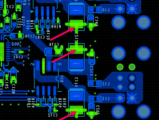
SHENZHEN HOYOGO ELECTRONIC TECHNOLOGY CO., LTD. is a professional manufacturer of high-precision double-sided, multilayer and impedance, blind buried vias, and thick copper circuit boards. Our products cover various circuit boards such as HDI, thick copper, backboard, rigid-flex, buried capacitance buried resistance, gold finger, etc., which can meet the needs of customers for various products.


 English
 Français
 Deutsch
 Português
 Pусский
 中文
中文