Welcome to visit Hoyogo website, let's connect the world together!
Customer service hotline:+86 13723413985 or 400 058 2288
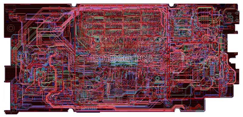
Circuit board design is a crucial part of the entire circuit board production, whether it is the design trend, the choice of ground point, the layout of power filter / decoupling capacitor, the line diameter, and the number of vias, solder joints and line density, these five key The point determines the final structure of the circuit board and the application quality.
1. Have a reasonable Direction
Such as input / output, AC / DC, strong / weak signal, high frequency / low frequency, high voltage / low voltage, etc.
2. Choose a good ground point: the ground point is usually the most important
We do not know how many engineers and technicians discussed this small ground point, which shows its importance. Due to various limitations, it is difficult to find a good grounding point, but you should try to follow it. This question is very flexible in practice. Everyone has their own set of solutions, which can be easily understood if it can be explained for a specific circuit board.
3. Choose a good ground point: the ground point is usually the most important
Usually, only a few power supply filter / decoupling capacitors are drawn in the schematic, but the location to be connected is not indicated. In fact, these capacitors are provided for switching devices or other components that require filtering / decoupling. These capacitors should be placed as close to these components as possible. If the capacitors are too far away from the components, they will be ineffective.
4. The diameter of the line requires that the size of the buried via and the through hole be appropriate
Conditional widening lines must not be too thin. The high-voltage and high-frequency lines should be smooth, without sharp chamfers, and no right angles should be used for turning. The ground wire should be as wide as possible, it is best to use a large area of copper, which has a considerable improvement in the problem of ground points. The size of the pad or wire hole is too small, or the size of the pad and the size of the drill hole are different. The former is not conducive to manual drilling, while the latter is not conducive to CNC drilling. It will be easy to drill the flash into a "c" shape, and in more serious cases, the pad will be drilled off. If the wire is too thin and there is no copper in a large area of the unrouted area, it is easy to cause uneven corrosion. That is, when the non-wiring area is corroded, the thin wires may be excessively corroded, or appear to be broken, or completely broken.
5. Number of vias, solder joints and linear density
It is not easy to find some problems in the early stage of circuit production. They tend to appear later, for example, there are too many wire holes, and the hidden dangers of the countersunk process will bury the hidden dangers. Therefore, the design should reduce the number of via holes as much as possible. The linear density in the same direction is too large, it is easy to connect them into one piece when welding. So, the linear density should be determined according to the welding process level. The welding spot distance is too small, which is not conducive to manual welding. We can only solve the welding quality problem by reducing the work efficiency, otherwise there will be hidden dangers.
Mastering the five key points of circuit board design can not only effectively improve the overall PCB production efficiency, but also protect product quality, save time, save manpower and material resources, reduce rework rates, and reduce material input costs.


 English
 Français
 Deutsch
 Português
 Pусский
 中文
中文