Welcome to visit Hoyogo website, let's connect the world together!
Customer service hotline:+86 13723413985 or 400 058 2288
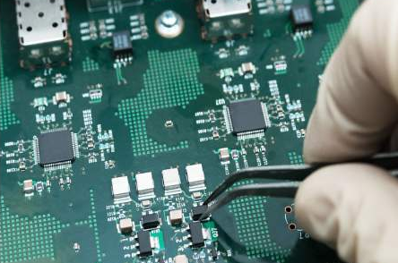
Electronic equipment needs high performance, high speed, thin, light and short, and PCB is a multidisciplinary industry and the most critical technology for high-end electronic equipment. The rigidity, flexibility, rigidity-flexibility of multi-layer boards in PCB products, as well as the module substrates used for IC packaging substrates, have made great contributions to high-end electronic equipment.
From the current PCB technology, we can see the following five development trends:
First: Development along the path of high-density interconnect technology (HDI)
Since HDI embodies the most advanced technology of contemporary PCBs, it can bring thin lines and small apertures to PCBs. Among HDI multilayer board application terminal electronic products, mobile phone is the model of HDI frontier development technology. In the fine wires of the PCB motherboard in mobile phones, the wire width/spacing has become mainstream. In addition, the thickness of the conductive layer and the board is thinner. The finer conductive pattern brings higher density and higher electronic device performance.
Second: Optoelectronic PCB has a bright future
It uses the optical path layer and the circuit layer to transmit signals. The key of this new technology is to manufacture the optical path layer (optical waveguide layer). It is an organic polymer formed by photolithography, laser ablation, reactive ion etching and other methods. At present, the technology has been industrialized in Japan and the United States.
Third: Component embedding technology
Semiconductor devices (called active components) and electronic components (called passive components) are formed on the inner layer of the PCB. Passive component function "component embedded PCB" has begun mass production, component embedded technology is a huge change in PCB functional integrated circuit, but to develop must solve the analog design method, production technology and inspection quality, reliability assurance is a top priority .
Fourth: The manufacturing process should be updated and advanced equipment should be introduced
HDI manufacturing has matured and tended to be perfect. With the development of PCB technology, although the commonly used subtractive manufacturing method still dominates in the past, low-cost processes such as additive and semi-additive methods have also begun to emerge. Secondly, nanotechnology is used to metalize the holes, at the same time to form PCB conductive patterns and a new method of manufacturing flexible boards.
Production of fine lines, new high-resolution photomasks and exposure equipment, and laser direct exposure equipment. Unified plating equipment. Equipment and facilities for the manufacture and installation of embedded production components (passive active components).
Fifth: PCB material development needs to be improved
Whether it is rigid or flexible PCB materials, for global lead-free electronic products, these materials must have higher heat resistance. So, new excellent materials with high Tg, small thermal expansion coefficient, small dielectric constant, and small dielectric loss are constantly emerging.


 English
 Français
 Deutsch
 Português
 Pусский
 中文
中文