Welcome to visit Hoyogo website, let's connect the world together!
Customer service hotline:+86 13723413985 or 400 058 2288
As data centers, cloud computing, and AI infrastructure continue to demand greater network bandwidth and data transmission capacity, 800G high-speed connectivity has been adopted in some high-performance data center switches, routers, and other high-speed networking equipment. Higher data rates impose stricter requirements on PCB materials, circuit fabrication, impedance control, and interlayer interconnections.
PCBs provide electrical connections and signal transmission paths for switch chips, high-speed interfaces, power circuits, and other functional modules. In 800G network equipment, PCB materials, stack-up construction, and manufacturing precision also need to meet product requirements related to high-speed signal integrity and power integrity. Different 800G network devices vary in port configuration, board architecture, interface type, and internal interconnection, so PCB materials, stack-up structures, and circuit configurations need to be determined according to specific product requirements.
HoYoGo is a professional 800G PCB manufacturer with high-reliability, high-precision, multilayer, and high-speed PCB manufacturing capabilities. As 800G network equipment places greater demands on high-speed signal transmission and long-term reliability, the following sections examine key PCB manufacturing considerations, including manufacturing precision, low-loss materials, interlayer interconnections, and back drilling.
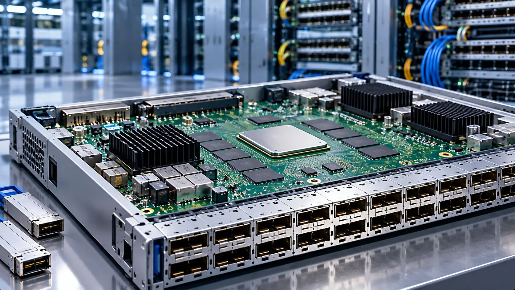
Manufacturing Precision Requirements for High-Speed Transmission
800G network equipment involves multichannel high-speed signal transmission. For controlled-impedance traces, trace width, differential-pair spacing, copper thickness, dielectric thickness, and material dielectric properties can affect the resulting impedance. Stack-up construction and dimensional variations during manufacturing may also affect high-speed signal transmission.
PCB manufacturing requires careful control of key parameters such as trace dimensions, trace compensation, copper thickness, dielectric thickness, and etching uniformity according to customer-specified stack-up structures, impedance targets, and technical requirements. Controlled-impedance traces should also be verified according to specified impedance targets and test conditions to ensure that actual impedance remains within the required range.
Low-Loss Materials and High-Speed Traces
High-speed signals traveling through a PCB are subject to both dielectric and conductor losses. For some 800G network equipment PCBs, factors such as dielectric constant (Dk), dissipation factor (Df), copper foil surface roughness, trace length, and dielectric thickness can affect transmission loss in high-speed traces. Signal integrity requirements for high-speed SerDes links also make parameters such as insertion loss, crosstalk, and impedance continuity important considerations.
Depending on trace structures, transmission distances, and product performance requirements, some 800G PCBs may use low-loss materials. Different materials vary in resin systems, dimensional stability, and processing characteristics. In production, the lamination, drilling, and circuit fabrication conditions need to be determined based on material characteristics. Attention should also be paid to the consistency of key parameters, including material electrical properties, Dk and Df stability, and dielectric thickness.
Multilayer Structures and High-Speed Interconnection
800G switches and routers typically need to interconnect high-speed interfaces, switch chips, power circuits, and other functional modules within limited board space. With an appropriate stack-up, multilayer PCBs can accommodate high-speed signal routing, power distribution, and interconnections between functional modules.
For PCBs with high routing density and complex interlayer interconnections, processes such as layer-to-layer registration, lamination, drilling, and hole metallization require consistent control. Some high-density products may also use HDI structures with microvias and other interlayer interconnection structures, depending on design requirements. For these PCBs, particular attention should be paid to hole position accuracy, laser drilling quality, hole metallization, and other critical manufacturing factors.
High-Speed Vias and Back Drilling
When high-speed signals travel between different PCB layers, vias are typically used to provide interlayer connections. For high-speed signal traces, unused portions of through-hole vias, known as via stubs, may cause reflections and affect signal transmission performance. Some PCBs used in 800G network equipment may require back drilling to remove the unused portions of plated through-hole vias. This shortens the via stubs and reduces their impact on high-speed signal transmission.
For PCBs requiring back drilling, key parameters such as back-drill depth, positional accuracy, and remaining stub length need to be controlled according to customer drawings, stack-up structures, and via design requirements. The back-drilling process also needs to match the PCB stack-up and target layer position to prevent drilling deviations from affecting high-speed via structures.
PCB Reliability Under Thermal Load
800G network equipment typically integrates high-speed switch chips, interface modules, and power components that generate heat under high-load operation. Overall heat dissipation depends primarily on the system's thermal design, but the thermomechanical properties of PCB materials, interlayer bonding, and via interconnection quality can also affect long-term reliability.
For PCBs exposed to elevated temperatures or temperature cycling over extended periods, materials should be selected according to product operating conditions and reliability requirements. Key manufacturing factors such as lamination quality, interlayer bonding, and plated hole quality also require careful control to reduce the risk of reliability issues such as delamination and barrel cracking. For high-reliability applications, material thermal expansion characteristics and structural stability under long-term thermal cycling should also be considered.
Volume Manufacturing and Consistency
Once 800G PCBs enter volume production, manufacturing consistency across different production batches becomes an important consideration. Variations in material properties, dielectric thickness, trace dimensions, copper thickness, and via structures can affect the impedance, dimensions, and electrical performance of finished PCBs.
From raw material management and inner- and outer-layer circuit fabrication to lamination, drilling, electroless copper deposition, electroplating, and final electrical testing, critical processes and manufacturing parameters need to be controlled according to product specifications. This helps maintain consistency in key parameters across production batches and allows finished PCBs to be checked against the applicable product specifications through the required inspections and tests.
From 800G to Higher Bandwidth
800G connectivity is already used in high-speed data center networks, while network interconnect technology continues to evolve toward 1.6T and higher bandwidth. Higher data rates and greater interconnection density place increasingly stringent requirements on PCB material selection, fine-line fabrication, multilayer lamination, impedance control, and complex via fabrication.
As demand grows for high-speed SerDes links and higher-frequency signal transmission, high-speed PCBs will require further advances in signal integrity control, low-loss material processing, and precision manufacturing. Because network equipment can differ in chips, interfaces, stack-up structures, and interconnection architectures, PCB manufacturers need to select suitable materials and determine the appropriate processing conditions according to product specifications and customer technical requirements.
HoYoGo is a professional 800G PCB manufacturer with expertise in multilayer, high-precision, and high-speed PCB manufacturing. To meet the signal transmission and manufacturing consistency requirements of 800G switches, routers, and data center networking equipment, we provide customized PCB manufacturing services based on each customer’s product specifications and technical requirements. Our production and quality control follow applicable IPC standards and customer specifications, helping customers bring their high-speed networking products to market.


 English
 Français
 Deutsch
 Português
 Pусский
 中文
中文