Welcome to visit Hoyogo website, let's connect the world together!
Customer service hotline:+86 13723413985 or 400 058 2288
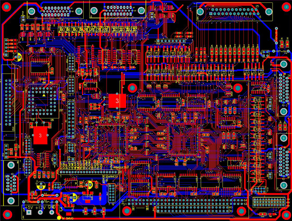
I. Impedance matching in PCB design
The design of PCB impedance matching refers to an appropriate matching method between the signal source or transmission line and the load.
According to the access method, there are 2 ways to design PCB impedance matching: serial and parallel.
According to the frequency of the signal source, the design of PCB impedance matching can be divided into 2 types: low frequency and high frequency.
In PCB design, high-frequency signals generally use serial impedance matching
The resistance range of the series resistance is 20~75Ω, and the resistance value is proportional to the signal frequency and inversely proportional to the PCB trace width. In the embedded system, serial matching resistances are generally required for signals with frequencies greater than 20M and PCB trace lengths greater than 5cm, such as clock signals, data and address bus signals in the system. There are two functions of series matching resistance:
1. Reduce high frequency noise and edge overshoot. If the edge of a signal is very steep, it contains a lot of high-frequency components, which will radiate interference and easily produce overshoot. The series resistance and the distributed capacitance of the signal line and the load input capacitance form an RC circuit, which will reduce the steepness of the signal edge.
2. Reduce high-frequency reflections and self-oscillation. When the frequency of the signal is high, the wavelength of the signal is very short. When the wavelength is as short as the length of the transmission line, the reflected signal superimposed on the original signal will change the shape of the original signal. If the characteristic impedance of the transmission line is not equal to the load impedance (mismatch), reflection will occur at the load end, causing self-oscillation. The low-frequency signal of the wiring in the PCB board can be directly connected, and it is generally not necessary to add a series matching resistances.
Parallel impedance matching is also called "terminal impedance matching"
Generally used at the input/output interface, mainly refers to the impedance matching with the PCB design of the transmission cable. For example, LVDS and RS422/485 use Category 5 twisted pair, the input end matching resistance is 100~120Ω. The matching resistance of the video signal using coaxial cable is 75Ω or 50Ω, and using flat cable is 300Ω. The resistance value of the parallel matching resistance is related to the medium of the transmission cable and has nothing to do with the length. Its main function is to prevent signal reflection and reduce self-excited oscillation.
It is worth mentioning that the impedance matching of PCB design can improve the EMI performance of the system. In addition, in order to solve the impedance matching of PCB design, in addition to using series/parallel resistances, transformers can also be used for impedance transformation. Typical examples are Ethernet interfaces and CAN buses, etc.
II, Zero ohm resistance
1. The simplest is to use as a jumper. If a certain section of the circuit is not used, just do not solder the resistance directly, which does not affect the appearance.
2. When the matching circuit parameters are uncertain, replace it with zero ohms. In actual debugging, determine the parameters first, and then replace them with specific numerical components.
3. When you want to measure working the current of a certain circuit, you can remove the zero ohm resistance and connect an ammeter. This is convenient for measuring current.
4. In the process of PCB design and layout, if you encounter problems that cannot be laid out, you can also add a zero ohm resistance to make a jumper.
5. In the high-frequency signal network, the zero ohm resistance acts as an inductor or a capacitor. This plays a role in the impedance matching of the PCB design, because zero-ohm resistance also has impedance.
When it acts as an inductor, it mainly solves the EMC problem.
6. Single-point grounding, such as the single-point docking of analog ground and digital ground.
7. It can be used for circuit configuration, which can replace jumper wire and DIP switches. Sometimes users will change the settings randomly, which is easy to cause misunderstanding. In order to reduce maintenance costs, zero-ohm resistances should be used instead of jumper wires and so on to be soldered on the board.
8. It can be used for system debugging. For example, divide the system into several modules, and separate the power and ground between the modules with a zero ohm resistance. When the power or ground is short-circuited during the debugging phase, removing the zero-ohm resistance can narrow the search range.
The above functions can also be replaced by "magnetic beads". Although zero-ohm resistance and magnetic beads are similar in function, there are essential differences. The former has impedance characteristics, and the latter has inductive reactance characteristics. Magnetic beads are generally used in power and ground networks for filtering.
SHENZHEN HOYOGO ELECTRONIC TECHNOLOGY CO., LTD. has a PCB design team with more than 12 years of work experience. We are not only proficient in using mainstream PCB design software in the market, but also can conduct professional and efficient communication to ensure the progress of PCB design. We are a professional PCB design company that can help customers in related industries seize market opportunities as early as possible.


 English
 Français
 Deutsch
 Português
 Pусский
 中文
中文