Welcome to visit Hoyogo website, let's connect the world together!
Customer service hotline:+86 13723413985 or 400 058 2288
In the specific PCB design process, the basic knowledge that needs to be mastered includes the following main parts:
1. Preparation
Including the preparation of component libraries and schematic diagrams. Before proceeding with PCB design, we must first prepare the schematic SCH component library and PCB component packaging library.
The PCB component package library is best established by the engineer based on the standard size data of the selected device. In principle, the PC component package library should be established first, and then the schematic SCH component library should be established.
Engineers have higher requirements for PCB component packaging library, because it will directly affect PCB installation; However, the requirements for the schematic SCH component library are relatively loose, but attention should be paid to defining the pin attributes and the corresponding relationship with the PCB component package library.
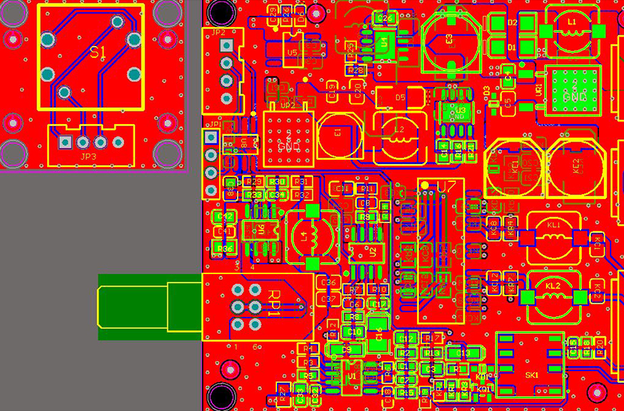
2. PCB Structure Design
According to the determined circuit board size and various mechanical positioning, draw the PCB frame in the PCB design environment, and place the required connectors, buttons/switches, screw holes, assembly holes, etc. according to the positioning requirements.
In addition, it is necessary to fully consider and determine the wiring area and non-wiring area, such as how much area around the screw hole belongs to the non-wiring area.
3. PCB Layout Design
The layout design is to place the components in the PCB frame according to the design requirements. Generate the netlist in the schematic tool (design→create netlist), and then import the netlist in the PCB software (design→import netlist). After the netlist is successfully imported, it will exist in the background of the software. Through the Placement operation, all the devices can be called out, and there is a flying line prompt connection between the pins. At this time, the layout design of the device can be carried out.
PCB layout design is the first important process in the entire PCB design process. The more complex the PCB board, the better the layout, the more directly affect the difficulty of the later wiring.
Layout design depends on the circuit board designer's basic circuit knowledge and rich design experience, which is a higher level requirement for the circuit board designer. Elementary circuit board designers have little experience, so they are suitable for small module layout design or PCB layout design tasks with lower overall board difficulty.
4. PCB Routing Design
PCB routing design is the process with the largest workload in the entire PCB design, which directly affects the performance of the PCB board.
In the PCB design process, wiring generally has 3 requirements:
The first is the layout, which is the most basic entry requirement for PCB design;
The second is the satisfaction of electrical performance, which is a standard to measure whether a PCB board is qualified. After the wiring is laid out, carefully adjust the wiring to achieve the best electrical performance;
The third is to keep the wiring neat and beautiful. If the wiring is disorderly, even if the electrical performance is passed, it will bring great inconvenience to the later modification of the board and test and maintenance. So the wiring must be neat and uniform, not criss-cross and disorderly.
5. Wiring Optimization and Silkscreen Placement
"PCB design is not the best, only better", "PCB design is an art of defects", this is mainly because PCB design needs to realize the design requirements of all aspects of hardware, and individual requirements may conflict with each other. You cant have your cake and eat it too.
For example: A certain PCB design project needs to be designed into a 6 layer board after evaluation by the circuit board designer. However, considering the cost of product hardware, it is recommended to design this project as a 4-layer board, so the signal shielding ground layer can only be sacrificed, which will increase the signal crosstalk between adjacent wiring layers and reduce the signal quality.
The general design experience is: the time to optimize the wiring is twice the time of the first wiring. After the PCB layout optimization is completed, post-processing is required. The first thing to do is the silkscreen logo on the PCB surface. The bottom silkscreen characters need to be mirrored during design to avoid confusion with the top silk screen.
6. Network DRC Inspection and Structure Inspection
Quality control is an important part of the PCB design process. General quality control methods include: design self-inspection, design mutual inspection, expert review meetings, special inspections, etc.
Schematic and structural element diagrams are the most basic design requirements. Network DRC inspection and structural inspection are to confirm that the PCB design meets the two input conditions of the schematic netlist and structural element diagram.
Generally, circuit board designers will have their own accumulated design quality inspection Checklist. Part of the items comes from the company or department's specifications, and the other part comes from their own experience summary.Special inspections include Valor inspection and DFM inspection of the design. These two parts focus on the PCB design output back-end processing gerber file.
7. PCB Manufacturing
Before the PCB is formally processed and manufactured, the circuit board designer needs to communicate with the PE of the PCB supplier to answer the manufacturer's confirmation questions about the PCB board processing.
This includes, but is not limited to: Selection of PCB base material model, adjustment of circuit layer line width and line spacing, adjustment of impedance control, adjustment of PCB stacking thickness, surface treatment processing technology, aperture tolerance control and delivery standards, etc.
SHENZHEN HOYOGO ELECTRONIC TECHNOLOGY CO., LTD. has a design team with more than 12 years of work experience. We are not only proficient in using mainstream PCB design software in the market, but also can conduct professional and efficient communication to ensure the progress of PCB design. We are a professional PCB design company that can help you seize market opportunities as early as possible.


 English
 Français
 Deutsch
 Português
 Pусский
 中文
中文