Welcome to visit Hoyogo website, let's connect the world together!
Customer service hotline:+86 13723413985 or 400 058 2288
In the manufacturing electronic equipment, PCB plays a vital role, and via holes are the bridge connecting different electronic layers. So can PCB via holes be made on the pad?
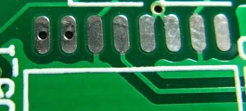
1. In the case of personal DIY, if the via hole is made on the pad, it may not cause big problem.
2. If such a method is used in the SMT production process, it may cause tombstone phenomenon. The reason is that the surface tension of the solder may cause components to stand up, causing problems such as virtual soldering, desoldering, and poor contact. Especially for the small package components, such as chip capacitors and chip resistors, the tombstone phenomenon is more likely to occur. In order to avoid this kind of situation occur, the pins of polygon pour are sometimes opening solder mask.
3. If the via holes are not properly plugged, it may lead to tin leakage and further cause the tombstone phenomenon. Therefore, the location of via holes also needs to be considered in terms of technology.
From the above 3 points, in order to ensure the reliability of the PCB and smooth progress of the technology, it is recommended to avoid directly drilling the via holes on the pads. However, under the following circumstances, drilling via holes on the pads is not a big problem and is acceptable.
Case 1:
If you are drilling holes on the back of a large pad, for example, drilling holes on the MOSFET pad to improve the heat dissipation of MOSFET pad to improve the heat dissipation of the MOSFET, this is okay. It should be noted that the via holes of large pads needs to be evenly distributed to ensure that the pads are evenly heated.
Case 2:
If it is necessary to drill via holes on the thermal pad, such as thermal via holes made to dissipate heat from the IC, since there are no pins that need to be soldered in the middle of the chip body, there is no need to consider issues such as tin leakage and virtual soldering in the via holes on the IC thermal pad.
In conclusion, whether via holes can be drilled on the PCB pad needs to be evaluated and decided based on specific requirements and technology conditions. At the same time, parameters such as the location, size, and quantity of via holes also need to be considered to meet circuit performance an reliability requirements. In actual operation, it is recommended to consult a professional PCB factory to obtain accurate advice and guidance.
HoYoGo is a professional and reliable PCB manufacturer. The management team has an average of 25 years of industry experience. We also have 2 factory production bases, with a monthly production capacity of 500,000sqm. With our own rich experience, production capacity and resources, we can provide you with one-stop service from small to large volume production.


 English
 Français
 Deutsch
 Português
 Pусский
 中文
中文