Welcome to visit Hoyogo website, let's connect the world together!
Customer service hotline:+86 13723413985 or 400 058 2288
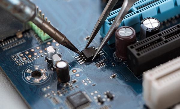
SHENZHEN HOYOGO ELECTRONIC TECHNOLOGY CO., LTD. specializes in providing overall PCBA electronics manufacturing services, including one-stop services from upstream electronic component procurement to PCB production and processing, SMT patch, DIP plug-in, PCBA testing and finished product assembly. The following is an introduction to everyone: the common causes of soldering defects in PCBA processing.
1. The solderability of the board hole affects the soldering quality
The poor solderability of the circuit board holes will cause PCBA processing and soldering defects, which will affect the parameters of the components in the circuit, resulting in unstable conduction between the components and the inner layer of the multilayer board, and the entire circuit function will fail. The so-called solderability refers to the property that the metal surface is wetted by molten solder, that is, a relatively uniform, continuous and smooth adhesive film is formed on the metal surface of the solder.
Main factors affecting the solderability of printed circuit boards:
(1) The composition of the solder and the properties of the solder. Solder is an important part of the welding chemical treatment process. It is composed of chemicals containing flux. Commonly used low melting point eutectic metals are Sn-Pb or Sn-Pb-ag. The impurity content should be controlled in a certain proportion. To prevent the oxides generated by impurities from being dissolved by the flux. The function of the flux is to help the solder to wet the surface of the soldered board by transferring heat and removing rust. Usually white rosin and isopropanol solvents are used.
(2) The bonding temperature and the cleanliness of the metal board surface also affect the solderability. When the temperature is too high, the solder spreading speed increases.
At this time, the activity is high, the circuit board and the melting surface of the solder are rapidly oxidized, causing solder defects, and the surface of the circuit board is contaminated, which also affects the solderability and causes defects. Including tin beads, tin balls, disconnection, poor gloss, etc.
2. Welding defects caused by warpage in PCBA processing
Circuit boards and components warp during welding, and stress deformation causes PCBA processing welding defects such as solder joints and short circuits. Warpage is often caused by temperature imbalance between the upper and lower parts of the board. For large PCBs, warpage may occur due to the weight of the board itself. Ordinary PBGA devices are about 0.5mm away from the printed circuit board. If the equipment on the circuit board is large, the circuit board will return to its normal shape after cooling, and the solder joints will be stressed for a long time.
3. PCB design affects soldering quality
In the PCB design layout, when the size of the circuit board is too large, although the soldering is easier to control, the printed line is long, the sensitivity increases, the noise resistance decreases, and the cost increases; If the temperature is too small, the heat dissipation will be reduced, the soldering will be difficult to control, and adjacent lines will easily occur.
Thus, the PCB design must be optimized:
(1) Shorten the wiring between high-frequency components to reduce electromagnetic interference.
(2) Parts with heavier weight (such as 20g or more) are fixed with brackets and then welded.
(3) Heat dissipation issues should be considered for heating components to prevent large defects and rework on the surface of the components. Thermal components should be kept away from heat sources.
(4) The arrangement of components should be as parallel as possible, which is beautiful and easy to weld, and should be mass produced. The board is designed as the best 4:3 rectangle. Do not change the line width to avoid intermittent wiring. When the board is heated for a long time, the copper foil is easy to expand and fall off. Please avoid using large area copper foil.
SHENZHEN HOYOGO ELECTRONIC TECHNOLOGY CO., LTD. has a professional design and development team. In addition to independent research and development of various PCB solutions, it also provides services to customers, such as assembly, PCB solution development, schematic design, PCB Layout routing, Bom list matching and component procurement.


 English
 Français
 Deutsch
 Português
 Pусский
 中文
中文