Welcome to visit Hoyogo website, let's connect the world together!
Customer service hotline:+86 13723413985 or 400 058 2288
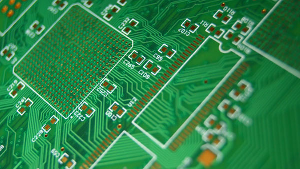
High-frequency circuits tend to have high integration and high routing density. The use of multi-layer boards is a must for routing, and it is also an effective way to reduce interference. In the PCB design stage, a reasonable choice of PCB size with a certain number of layers can make full use of the intermediate layer to set up the shield to better realize the nearest grounding, and effectively reduce the parasitic inductance and shorten the signal transmission length. At the same time, it can greatly reduce signal cross-interference. These methods are beneficial to the reliability of high frequency circuits.
With using the same material, the noise of the 4-layer board is 20DB lower than that of the double-sided board. But there is also a problem: the higher the number of PCB layers, the more complicated the manufacturing process and the higher the cost. This requires that in the PCB design, in addition to selecting the appropriate number of layers of the PCB board, it is also necessary to carry out a reasonable layout plan of the components and adopt the correct routing rules to complete the design.
1. The alternation of lead layers between pins of high-frequency circuit devices should be reduced.
This means that the fewer vias used in the component connection process, the better. A via can bring about 0.5pF distributed capacitance, reducing the number of vias can significantly increase the speed and reduce the possibility of data errors.
2. The leads between the pins of high-frequency circuit devices should be shortened.
The radiation intensity of the signal is proportional to the trace length of the signal line. The longer the high-frequency signal lead, the easier it is to couple to the components close to it, so it is required for high-frequency signal lines such as signal clock, crystal oscillator, DDR data, LVDS line, USB line, HDMI line, etc. Keep the traces as short as possible.
3. Lead bending between pins of high-speed electronic devices should be reduced.
It is best to use a full straight line for the routing of the high-frequency circuit. When the lead needs to be bent, it can be bent with a 45-degree fold line or a circular arc. This requirement is only used to improve the fixing strength of copper foil in low-frequency circuits, but meeting this requirement in high-frequency circuits can reduce the external emission and mutual coupling of high-frequency signals.
4. Please pay attention to the "crosstalk" introduced by the signal lines in parallel routing at close distances.
When we are routing high-frequency circuits, we should pay attention to the "crosstalk" introduced by the signal lines in close parallel routing. Crosstalk refers to the coupling phenomenon between signal lines that are not directly connected. Since high-frequency signals are transmitted along the transmission line in the form of electromagnetic waves, the signal line will act as an antenna, and the energy of the electromagnetic field will be emitted around the transmission line. The parameters of the PCB layer, the spacing of the signal lines, the electrical characteristics of the driving end and the receiving end, and the signal line termination method all have a certain impact on the crosstalk. So, in order to reduce the crosstalk of high-frequency signals, it is required to do the following as much as possible when wiring:
(1) If the routing space permits, insert a ground wire or ground plane between the two wires with more serious crosstalk, which can play a role in isolation and reduce crosstalk;
(2) Under the premise that the routing space permits, the spacing between adjacent signal lines should be increased, and the parallel length of the signal lines should be reduced. The clock line should be as perpendicular to the key signal line as possible instead of parallel;
(3) If parallel routing in the same layer is almost unavoidable, then the routing directions of the two adjacent layers must be perpendicular to each other;
(4) In digital circuits, the usual clock signals are signals with fast edge changes, so the external crosstalk is large. So, in the design, the clock line should be surrounded by a ground wire and more ground wire holes should be used to reduce the distributed capacitance, thereby reducing crosstalk;
(5) For high-frequency signal clocks, low-voltage differential clock signals should be used as much as possible to wrap the ground mode, and attention should be paid to the integrity of the ground punching;
(6) Please do not leave unused input terminals in the air, it needs to be grounded or connected to the power supply. Because the dangling wire may be equivalent to the transmitting antenna, the grounding can suppress the emission.
SHENZHEN HOYOGO ELECTRONIC TECHNOLOGY CO., LTD. has a PCB design team with more than 12 years of work experience. We are not only proficient in using mainstream PCB design software in the market, but also can conduct professional and efficient communication to ensure the progress of PCB design. We are a professional PCB design company that can help customers in related industries seize market opportunities as early as possible.


 English
 Français
 Deutsch
 Português
 Pусский
 中文
中文