Welcome to visit Hoyogo website, let's connect the world together!
Customer service hotline:+86 13723413985 or 400 058 2288
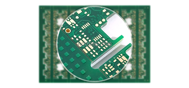
Vias are one of the important components of multilayer PCBs. The cost of drilling usually accounts for 30% to 40% of PCB manufacturing costs. Simply put, each hole on the PCB can be called a via.
First: Parasitic Capacitance of Via
The via itself has a parasitic capacitance to ground. If the diameter of the isolation hole of the via on the ground layer is known to be D2, the diameter of the via pad is D1, and the thickness of the PCB board is T, and the dielectric constant of the board substrate is ε, the parasitic capacitance of the via hole is approximately: C = 1.41εTD1/(D2-D1).
The main effect of the parasitic capacitance of the via on the circuit is to extend the rise time of the signal and reduce the speed of the circuit. For example, for a PCB with a thickness of 50Mil, if a via with an inner diameter of 10Mil and a pad diameter of 20Mil is used, and the distance between the pad and the ground copper area is 32Mil, then we can approximate the via through the above formula: the parasitic capacitance is roughly:
C=1.41x4.4x0.050x0.020/(0.032-0.020)=0.517pF.
The rise time change caused by this part of the capacitor is: T10-90 = 2.2C (Z0 / 2) = 2.2x0.517x (55/2) = 31.28ps.
From these values, it can be seen that although the effect of slowing the rise delay caused by the parasitic capacitance of a single via is not very obvious. However, if vias are used multiple times to switch between layers, designers still need to consider carefully.
Second: The Parasitic Inductance of the Via
Similarly, parasitic capacitance and inductance exist in the via. In the design of high-speed digital circuits, the harm caused by the parasitic inductance of the via hole is usually greater than the effect of the parasitic capacitance. Its parasitic series inductance will weaken the role of bypass capacitors and weaken the filtering effect of the entire power system. We can use the following formula to simply calculate the approximate parasitic inductance of the via: L = 5.08h [ln(4h / d)+1]. Where L is the inductance of the via, h is the length of the via, and d is the center diameter. It can be seen from the formula that the diameter of the via has little effect on the inductance, while the length of the via has the greatest influence on the inductance. Still using the above example, the inductance of the via can be calculated as: L = 5.08x0.050 [ln(4x0.050 / 0.010)+1] = 1.015nH. If the rise time of the signal is 1 ns, the equivalent impedance is: XL =πL/ T10-90 =3.19Ω. This kind of inductance can no longer be ignored when passing high-frequency currents. It is important to note that the insertion capacitor needs to pass through two vias when connecting the power layer and the ground layer, so that the parasitic inductance of the vias will multiply.
Third: Via design in high-speed PCB
Through the above analysis of the parasitic characteristics of vias, we can see that in high-speed PCB design, the seemingly simple vias usually also bring a great negative impact on the circuit design. In order to reduce the adverse effects caused by the parasitic effects of vias, in the design, you can do as much as possible:
1. Considering the cost and signal quality, please choose a via of reasonable size. For example, for the design of the 6-10 layer memory module PCB, it is best to use 10/20Mil (drilled hole/pad) vias. For some high-density small size boards, you can also try to use 8/18Mil hole. Under the current technical conditions, it is difficult to use through holes of a smaller size. For vias for power or ground, consider using larger sizes to reduce impedance.
2. The two formulas discussed above can be concluded that the use of thinner PCB boards is beneficial to reduce the two parasitic parameters of vias.
3. The power supply and ground pin should be drilled into the nearest hole. The lead between the hole and the pin should be as short as possible because they increase inductance. The power and ground leads should be as thick as possible to reduce impedance.
4. The signal traces on the PCB should not change the layers as possible, that is, try not to use unnecessary vias.
5. Place some grounded vias near the vias for signal changeover to provide the closest loop for the signal. You can even place a lot of extra ground vias on the PCB.
HOYOGO is an international, professional, reliable PCB manufacturer. We have 2 production bases with a monthly production capacity of 500,000 square meters. One-stop PCB product supply and solution. And HOYOGO have a management team with 25 years of average industry experience and reliable quality assurance.


 English
 Français
 Deutsch
 Português
 Pусский
 中文
中文