Welcome to visit Hoyogo website, let's connect the world together!
Customer service hotline:+86 13723413985 or 400 058 2288
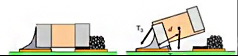
The tombstoning phenomenon refers to the phenomenon that one end of the electronic component does not touch the pad and stands obliquely upwards or the contact pad is upright during PCBA processing. So how to avoid this phenomenon?
1. Warm-up Period
We should correctly set the technology parameters during preheating. When the preheating temperature is set low and the preheating time is set short, the probability of melting the solder paste at both ends of the component at the same time will greatly increase, resulting in unbalanced tension at both ends, thus forming a "tombstoning".
2. Pad Size
When designing chip resistor and capacitor pads, the overall symmetry should be strictly maintained, that is, the shape and size of the pad pattern should be exactly the same to ensure that the resultant force acting on the solder joints on the component is zero when the solder paste melts, so that forming ideal solder joints.
For small thin chip components, please do not design with different pad sizes, or connect one end of the pad to the ground plane, which may cause tombstoning of the component. During reflow, the component nearly floats on the liquid solder and reaches its final position as the solder solidifies. Using pads of different sizes can result in an imbalance in the flow time of the solder paste as the pads heat up, resulting in tombstoning.
3. Solder Paste Thickness
When the thickness of the solder paste is thinner, the surface tension will decrease when the solder paste melts, and the heat capacity of the entire pad will also decrease, and the probability of simultaneous melting of the solder paste on the two pads will also increase. So, as the thickness of the solder paste becomes smaller, the probability of tombstoning is greatly reduced.
4. Mounting Offset
Generally, during the reflow melting process of solder paste, due to the surface tension, the component deviation generated during the installation process will be automatically corrected by pulling the component. But if the offset is severe, pulling will cause the component to tombstone. Because the solder end that is in more contact with the component gets more heat capacity, it will melt first. Therefore, it is necessary to adjust the placement accuracy of components to avoid large placement deviations.
5. Component Weight
Lighter components have a higher incidence of tombstoning because unbalanced tension tends to pull the component, so when selecting components, larger size and weight components should be given priority.
Different welding defects have different solutions, and they often restrict each other. For example, increasing the preheat temperature can effectively eliminate the tombstoning phenomenon, but the heating rate is faster and may produce a large number of solder balls. Therefore, when solving welding defects, we should consider many aspects and choose a compromise solution.
SHENZHEN HOYOGO ELECTRONIC TECHNOLOGY CO., LTD. is a company specializing in providing PCBA electronic overall manufacturing services, including one-stop services from upstream electronic components procurement to PCB production and processing, SMT placement, DIP plug-in, PCBA testing, and finished product assembly.


 English
 Français
 Deutsch
 Português
 Pусский
 中文
中文