Welcome to visit Hoyogo website, let's connect the world together!
Customer service hotline:+86 13723413985 or 400 058 2288
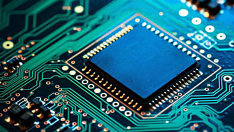
As a support body for electronic components, PCB is crucial to ensuring the normal operation of the entire system. When doing PCB prototyping, choosing appropriate specifications is very critical, which directly affects the performance, stability and reliability of the PCB. So, how to choose the best PCB proofing specifications?
1. Base Material Type
The choice of material has a direct impact on PCB performance. Common PCB materials include FR-4, aluminum, polyimide (PI), etc. Different materials have different electrical properties, thermal conductivity properties and mechanical strength, so the appropriate material needs to be selected based on specific needs.
2. Number of Layers
The selection of the number of PCB layers is also a crucial specification. Different application scenarios require different number of layers of circuit boards. An increase in the number of layers can provide more layout space, making the circuit board more compact and flexible. However, as the number of layers increases, so does the manufacturing cost and complexity, thus requiring trade-offs in the design.
3. Conventional Technologies
There are many conventional technologies for PCB. The PCB prototyping specifications shown below should be helpful.
1) Solder mask color: There are various colors such as green, blue, black, red, yellow, etc., but the most used one is green.
2) There are many options for PCB board thickness: The conventional first choice is 1.6mm. Of course, there are also different thicknesses such as 0.8mm, 1.0mm, 1.2mm, 1.6mm and 2.0mm for you to choose from. If you have no special requirements, it is recommended to choose 1.6mm.
3) When selecting the copper foil thickness, it should be determined according to the power of the equipment. The commonly used copper foil thickness is 1OZ. If the equipment has higher power, you can choose thicker copper foil to ensure good heat dissipation performance.
4) Character color is also called silk screen color. White is the most common because it forms a strong contrast with the green solder mask and can be displayed more clearly. Of course, other colors can also be used for silk screen printing, but it is recommended to choose a color that has high contrast with the solder mask color.
5) State of the Via hole, mainly including vias with solder mask opening, vias covered with solder mask ink, and vias plugging.
Vias with Solder Mask Opening: Open solder mask where there are vias to expose the copper foil at both ends of the vias.
Vias Covered with Solder Mask Ink: There is no solder mask opening, green solder mask ink covers the copper foil at both ends of the via.
Vias Pugging: Filling vias by using green solder mask ink, resin, metal and other materials.
6) In addition, there are specifications such as minimum width/spacing, minimum hole size, etc. The smaller these specifications are, the higher the difficulty. You can choose based on the process capabilities provided by the manufacturer.
4. Surface Finishing
Because the copper solder joints on the circuit board are easily oxidized when exposed to the air, causing problems such as poor contact and other problems, it is very necessary to do surface finishing.
Surface finishing technologies include HASL, HASL Lead Free, immersion gold, electroplating gold, OSP, etc. You can choose a reasonable technology based on your needs.
1) HASL and HASL Lead Free technology are mature and low cost.
2) Immersion gold means plating gold on PCB, and the whole process undergoes a chemical reaction, so it is also called ENIG. The surface of the board after immersion gold is smooth and the color is stable.
3) OSP, Organic Solderability Protective, is the lowest cost among PCB surface finishing technologies.
There are other special technologies in PCB production and manufacturing. Although they are rarely used, there is demand in the market, so they are classified as special technologies, such as gold fingers, blind and buried vias, multi-layer special stacked structures, ENEPIG, etc.
HoYoGo is an international, professional and reliable PCB manufacturer. We have our own factories, advanced machines and excellent quality system. We can also provide you with preferential prices for metal materials, support various complex technologies, customize your products according to your requirements. If you have related needs, you are welcome to send us your inquiries.


 English
 Français
 Deutsch
 Português
 Pусский
 中文
中文