Welcome to visit Hoyogo website, let's connect the world together!
Customer service hotline:+86 13723413985 or 400 058 2288
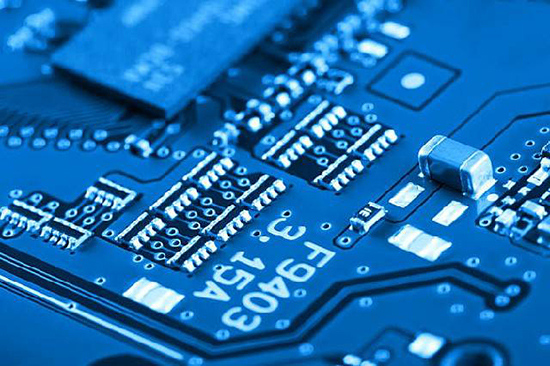
In the PCB manufacturing process, the lamination technology is the most important step. Some quality defects may occur during this process, which will affect the quality of the final PCB product. So what causes the defects? How do we solve these defects?
1. After the lamination of multi-layer boards is completed, if chronic misalignment occurs, it is not in the board material parts of the inner layer boards.
Reason 1: The positioning pin is too short and the position is inaccurate.
Solution: Use longer plugs instead.
Reason 2: The small size of the positioning pin causes looseness with the positioning hole of the base material.
Solution: ①Replace with new pins. ②Trim the problematic positioning pin.
Reason 3: Regarding the position of the tooling hole, the circular shape of the inner film has been aliased.
Solution:
①First put the inner films together, then check their upper and lower alignment, and replace the misaligned inner films.
②Strengthen on-the-job training for relevant operators.
Reason 4: The tooling holes of each inner layer board cannot be aligned and passed through, and the stacked template cannot be aligned.
Solution: Redo the tooling holes of the inner boards.
Reason 5: The tooling hole of the inner thin board is torn or deformed.
Solution: Before etching, additional copper surface for stiffener should be reserved around the tooling hole to reduce hole shape variation.
Reason 6: The high pressure exerted at high temperature causes the inner thin board to deform.
Solution:
①Recheck the pressure intensity used. It is necessary to find multiple appropriate values according to the size and thickness of the board, rather than using only a single data.
②Pay attention to whether the numerical surface pressure is correct and whether the press operation is standardized.
③Use a lower pressure intensity for the thin board without affecting the glue flow of the prepreg.
④Use a tool tip with a thicker diameter instead.
⑤Check the parallelism and flatness of the upper and lower hot pads.
2. Dimples and depressions appear on the outer copper surface after lamination.
Reason 1: Poor lamination and lamination environment.
Solution:
①Lamination work should be performed in a cleanroom environment.
②The inner layer board and prepreg must undergo antistatic treatment to reduce the adsorption of dust and debris.
③Wipe the surface of the steel plate with an anti-static dust-removing cloth.
Reason 2: Defects appears on the surface of the steel plate
Solution:
①Wipe the surface of the steel plate regularly with an anti-static dust-removing cloth.
②Hold the steel plate carefully to prevent surface damage.
③Do not use steel plates with serious surface defects.
3. Glue spots appear on the outer copper surface after lamination.
Reason: The resin falls off from the loose edges of the prepreg during lamination, causing surface contamination of the copper surface.
Solution:
①Lamination work must be carried out in a cleanroom.
②Cutting of prepreg and punching of tool holes must be done at points outside the dust-free lamination area.
③Use a heat gun to quickly hot melt the cut prepreg around the edges to prevent the prepreg from falling off.
4. The whole batch of finished boards are of different thickness
Reason 1: A mix of prepregs from different brands was used.
Solution:
①For multi-layer board materials with strict thickness tolerance requirements, be sure not to mix prepregs of different brands.
②Avoid using prepregs from different sources in a single board.
③Narrow the tolerance range of prepreg size.
Reason 2: The lamination process is not stable enough.
Solution:
① Optimize and standardize the lamination process.
② Strengthen on-the-job training.
5. Irregular and locally thicker differences appear on the board surface after pressing
Reason 1: The prepreg has too much glue content, and irregular thick spots and even holes often appear in the copper-free areas with low inner flow.
Solution: Some non-functional copper can be deliberately left in the large area of bare board in the inner layer as a buffer to make the pressure uniform.
Reason 2: The fiberglass cloth on the inner copper surface is too thick or the glue flow is insufficient, which not only causes local thickening, but may also cause white spots.
Solution:
① It can be replaced by PP with high glue content.
② Remove the non-functional residual copper surface as much as possible to avoid the board surface being too thick.
HoYoGo is a professional and reliable PCB manufacturer, including one-stop services from upstream electronic component procurement to PCB production and processing, SMT placement, PCBA testing, and finished product assembly, etc. All of our products strictly follow the acceptance standards of IPC-A-600-H and IPC-6012. We do not relax any step of inspection, to ensure the quality of customers, so that customers can rest assured of us.


 English
 Français
 Deutsch
 Português
 Pусский
 中文
中文