Welcome to visit Hoyogo website, let's connect the world together!
Customer service hotline:+86 13723413985 or 400 058 2288
I. Enhance the ability of PCB to resist deformation
The deformation of the circuit board is usually comes from rapid thermal expansion and contraction caused by high-temperature reflow, coupled with uneven distribution of parts and copper foil on the circuit board, which will aggravate the deformation of the circuit board.
The methods to increase the resistance to deformation of the circuit board are:
1. Increase the thickness of the PCB circuit board. If possible, it is recommended to use a circuit board with a thickness of 1.6mm or greater.
2. Use high Tg PCB material.
3. Pour glue on the circuit board. You can also consider pouring glue around the BGA or the back of the corresponding circuit board to enhance its stress resistance.
4. Add reinforcement around the BGA. If there is space, you can consider building a supporting iron frame around the BGA to strengthen its ability to resist stress, just like building a house.
II. Reduce PCB deformation
Generally speaking, when the circuit board is assembled into the case, it should be protected by the case, but because today's products are getting thinner and thinner. In particular, handheld devices often deform the circuit board due to external force bending or drop impact.
In order to reduce the deformation of the circuit board due to external forces, the following methods can be used:
1. Strengthen the shell to prevent its deformation from affecting the internal circuit board.
2. Add screws or positioning and fixing mechanisms around the BGA in the printed circuit board. If it is only for the purpose of protecting the BGA, the components near the BGA can be forcibly fixed to prevent deformation near the BGA.
3. Increase the buffer design of the mechanism to the circuit board. For example, when designing some buffer materials, even if the case is deformed, the internal circuit board can still remain unaffected by external stress. But the life and capacity of the buffer material must be considered.
III. Enhance the reliability of BGA
1. Fill the bottom of the BGA with glue.
2. Use SMD (solder mask design) layout. Cover the solder pads with green paint.
3. Increase the amount of solder. But it must be controlled under the condition that do not allow short circuits.
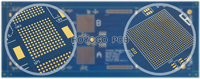
4. Increase the size of the BGA pads on the circuit board. This will make the wiring of the circuit board difficult, because the gap between the ball and the ball that can be routed becomes smaller.
5. Use Vias-in-pad design. However, the holes on the pads must be electroplated, otherwise bubbles will be generated during reflow, which can easily cause the solder balls to crack from the middle.
SHENZHEN HOYOGO ELECTRONIC TECHNOLOGY CO., LTD. is a manufacturer specializing in the production of high-precision double-sided, multilayer and impedance, blind buried vias, thick copper circuit boards. The products cover various circuit boards such as HDI, thick copper, backboard, rigid-flex combination, embedded capacitors, gold fingers, etc., which can meet the needs of customers for various products.


 English
 Français
 Deutsch
 Português
 Pусский
 中文
中文