Welcome to visit Hoyogo website, let's connect the world together!
Customer service hotline:+86 13723413985 or 400 058 2288
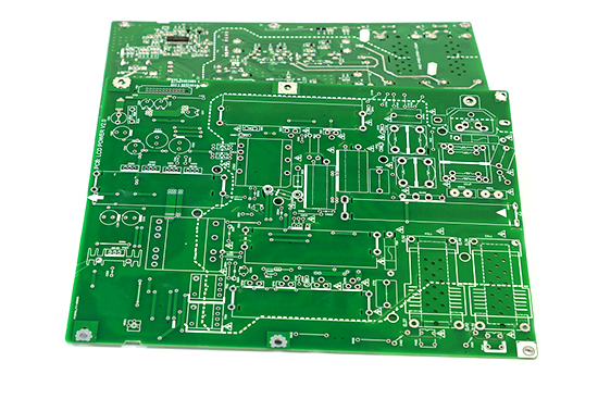
Do you know that PCB has pattern plating and tenting process? How to choose between them? Don't worry, let's first understand what are PCB pattern plating and tenting? In PCB manufacturing, pattern plating and tenting refer to two different graphic processing methods used by PCB factory when making photolithography patterns.
Next, let's take a look at two different graphics processing methods used in photolithography patterns:
Pattern plating process: the pattern is positive!
The pattern plating process means that PCB factory transfer the design pattern directly to the photoresist when making photolithography patterns, and then expose the photoresist part to the light source by photolithography. In this way, the photoresist will retain the area that matches the design pattern during the development process, forming the pattern of wires and components.
Tenting Process: Patterns are mirrored!
The tenting process is the opposite process. When making photolithographic patterns, PCB factory transfer the reverse (mirror image) of the design pattern to the photoresist, and then expose the part of the photoresist to the light source by photolithography. During development, the photoresist leaves areas that match the direction of the designed pattern, the opposite of the circuit pattern.
Finally, let's learn about their respective advantages:
PCB Pattern Plating:
1. Simplify the design process: The pattern plating process uses the positive direction of the design pattern to be consistent with the circuit diagram, making the manufacturing process more intuitive and direct.
2. Accuracy and reliability: The pattern plating process can accurately reproduce the design pattern, ensuring the accuracy of circuit connection and component layout, thus providing more reliable circuit performance.
3. Wide applicability: The pattern plating process is suitable for the manufacture of most conventional circuit boards, especially boards with no special requirements or special types.
PCB Tenting:
1. Special needs: The tenting process is suitable for special types of circuit board manufacturing.
2. Flexibility: By using the tenting process, the pattern opposite to the pattern plating process can be realized to meet the needs of special designs or specific functions.
3. Cost-Effectiveness: In some cases, the tenting process may be more cost-effective as it can reduces certain steps and material usage in the production process.
We learned about the two different patterning methods used in making photolithography patterns and their respective advantages. Now, do you know how to choose PCB pattern plating and tenting?
It doesn’t matter if you still don’t know how to choose. HoYoGo is a professional PCB factory with rich experience in PCB production, if you have any questions, welcome to consult.


 English
 Français
 Deutsch
 Português
 Pусский
 中文
中文