Welcome to visit Hoyogo website, let's connect the world together!
Customer service hotline:+86 13723413985 or 400 058 2288
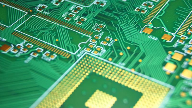
When we are doing electromagnetic compatibility in PCB design, we must take measures such as anti-interference and shielding of line signals. Otherwise, it is likely to cause signal crosstalk between lines. So how do we carry out reasonable routing? How to design electromagnetic compatibility?
1. Suitable wire width
The width of the wire will affect the electromagnetic compatibility of the PCB. When we choose the wire width, we must be able to ensure the electrical performance and ease of production, usually determined by the minimum current value that can withstand. In order to reduce the electromagnetic interference impact caused by the transient current on the PCB, the line width is controlled in the PCB design. Transient interference is generally caused by the inductance of the wire, and its inductance is directly proportional to the length of the wire and inversely proportional to the line width. For signal lines that often have large transient currents, short and wide wires should be used. If the layout space permits, a grid-shaped layout structure can be adopted.
2. Component routing
Routing will also affect PCB electromagnetic compatibility. When we are routing, we should try to put the devices that are closer to the routing together, the layout of the high-speed lines should be as short as possible, and the power devices and small-signal devices should be laid out separately. We should also pay attention to whether the design of the placement location is beautiful and tidy, whether it is convenient for function testing, the use of later interface and connections. In high-speed systems, the propagation delay of grounding lines and interconnecting lines is also a design factor that we need to consider. The transmission time of the signal transmission line has a great influence on the operating speed of the overall PCB system. If a common interconnection line is used where a high-speed line is used, it will increase the delay time and reduce the system operating speed.
3. Routing rules for high-frequency and high-speed signals
Generally, equal routing can reduce the inductance between wires, but in order to suppress the crosstalk of PCB wires, we should try to avoid long-distance equal routing when designing the routing. When designing restraint wires, please avoid sharp turns, and try to make the equidistant routing have a certain radian curve. There are high-current components on the PCB, please try to connect the ground wire separately to avoid noise interference. Set a ground wire between small signal or sensitive signal wires. The high-speed signal adopts the differential signal routing design, so that the positive and negative two differential lines are always coupled to each other on the transmission line, which can effectively reduce the electrical noise effect of the signal.
SHENZHEN HOYOGO ELECTRONIC TECHNOLOGY CO., LTD. has a PCB design team with more than 12 years of work experience. We are not only proficient in using mainstream PCB design software in the market, but also can conduct professional and efficient communication to ensure the progress of PCB design. We are a professional PCB design company that can help customers in related industries seize market opportunities as early as possible.


 English
 Français
 Deutsch
 Português
 Pусский
 中文
中文