Welcome to visit Hoyogo website, let's connect the world together!
Customer service hotline:+86 13723413985 or 400 058 2288
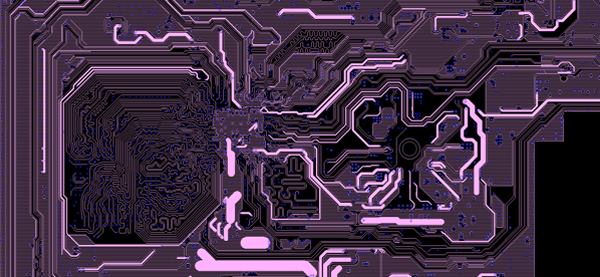
In the PCB layout process, after completing the system planning, the PCB diagram should be checked to see whether the system planning is reasonable and whether the best results can be achieved.
1. System planning ensures whether the wiring is reasonable or optimal, whether the wiring can be carried out reliably, and whether it can ensure the reliability of circuit operations. When planning, it is necessary to have an overall understanding and planning of the direction of the signal and the power and ground wire network.
2. Whether the size of the circuit board matches the size of the processing drawings, whether it can meet the technical requirements of PCB production and whether there are behavior symbols. It is important to note that the circuit planning and wiring of many PCB boards have been carefully planned and reasonably designed, but the precise positioning of the positioning connectors has been ignored, resulting in the planned circuit cannot be connected to other circuits.
3. Whether the components conflict in two-dimensional and three-dimensional space. Please pay attention to the actual size of the device, especially the height of the device. When welding components that are free of planning, the height usually cannot exceed 3mm.
4. Whether all the components are placed in an orderly and regular manner. When planning the components, not only the direction of the signal and the type of the signal should be considered, but also the overall density of the equipment planning should be considered in the case of maintenance, so that the density is even.
5. Whether the components that need to be replaced frequently can be easily replaced, and whether the plug-in board can be easily inserted into the device. It is also necessary to ensure the convenience and reliability of the replacement and plug-in of frequently-changed components.
6. Whether it is convenient to adjust the adjustable parts.
7. Whether there is a proper distance between the thermal element and the heating element.
8. Whether there is a radiator or electric fan installed in the place where heat dissipation is needed, and whether the air flow is unobstructed. Please pay attention to the heat dissipation of components and circuit boards.
9. Whether the signal direction is smooth and whether the interconnection is the shortest.
10. Whether the plug, socket, etc. are in opposition to the mechanical planning.
11. Whether the interference of the circuit board have been considered.
12. Whether the mechanical strength and function of the circuit board have been considered.
13. The art and beauty of circuit board planning.
SHENZHEN HOYOGO ELECTRONIC TECHNOLOGY CO., LTD. is a professional manufacturer specializing in the production of various high-end single-sided, double-sided, multilayer printed circuit boards and various special material PCBs. At the same time, in order to better serve customers, the company established a PCB design and development team in October 2018. In addition to independent research and development of various PCB solutions, we can also provide customers with a full range of value-added services: including SMT assembly, PCB program development, schematic design, PCB Layout and routing, Bom list matching, component procurement and other services.


 English
 Français
 Deutsch
 Português
 Pусский
 中文
中文