Welcome to visit Hoyogo website, let's connect the world together!
Customer service hotline:+86 13723413985 or 400 058 2288
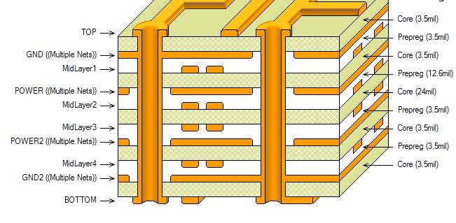
In PCB design, considering the signal quality control factors, the general principle of PCB stack-up is as follows:
1. The second layer adjacent to the component surface is the ground plane, which provides a device shielding layer, and the top-level wiring provides a reference plane.
2. All signal layers are as close as possible to the ground plane to ensure a complete return path.
3. Please try to avoid two signal layers directly adjacent to reduce crosstalk.
4. The main power supply is as close as possible to form a plane capacitor to reduce the power plane impedance.
5. Taking into account the symmetry of the laminated structure, it is beneficial to the warpage control in the plate making process.
The above are the general principles of stack-up design. In the actual stack-up of layered design, the circuit board designers can reduce the distance between the corresponding wiring layer and the reference plane by increasing the distance between adjacent wiring layers, thereby controlling the crosstalk rate of wiring between layers, and it is possible to use two signal layers directly adjacent to each other. For consumer products that pay more attention to cost, the way in which the power and ground layers are adjacent to the plane impedance can be weakened, thereby reducing the wiring layer as much as possible and reducing the PCB cost. Of course, there is a risk of signal quality design in doing so.
For the backplane stack-up design, in view of the common backplane, it is difficult to achieve adjacent wiring perpendicular to each other, so parallel long-distance wiring will inevitably appear. For high-speed backplanes, the general stack-up principle is as follows:
1. The top and bottom surfaces are complete ground planes, forming a shielded cavity.
2. There is no parallel wiring of adjacent layers to reduce crosstalk, or the distance between adjacent wiring layers is much larger than the reference plane distance.
3. All signal layers are as close as possible to the ground plane to ensure a complete return path.
It should be noted that in a specific PCB stack-up setting, the above principles should be designed and used flexibly, and a reasonable analysis should be carried out according to the actual single board requirements.
In order to better serve customers, HOYOGO established a PCB design and development team in October 2018. In addition to independent research and development of various PCB solutions, we can also provide customers with a full range of value-added services: including SMT assembly, PCB program development, schematic design, PCB Layout and routing, Bom list matching, component procurement and other services.


 English
 Français
 Deutsch
 Português
 Pусский
 中文
中文