Welcome to visit Hoyogo website, let's connect the world together!
Customer service hotline:+86 13723413985 or 400 058 2288
SHENZHEN HOYOGO ELECTRONIC TECHNOLOGY CO., LTD. has a PCB design team with more than 12 years of work experience. We are not only proficient in using mainstream PCB design software in the market, but also can conduct professional and efficient communication to ensure the progress of PCB design. We are a professional PCB design company that can help customers in related industries seize market opportunities as early as possible.
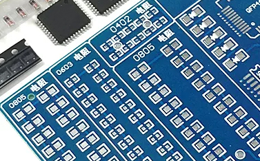
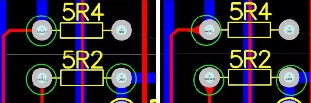
What is pad?
The pad is the basic unit of the surface mount component, used to form the land pattern of the circuit board, that is, various land combinations designed for special component types. The pad is used for electrical connection, device fixing, or part of the conductive pattern that combines both.
Pad type in PCB design:
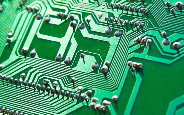
I. Common Pad
1. Square Pad--This type of pad is usually used when the printed circuit board components are large and few, and the printed wires are simple. It is easier to use this kind of pad when making PCB by hand.
2. Round Pad--This type of pad is widely used in single and double-sided printed boards with regularly arranged components. If the density of the board allows, the pad can be larger so that it will not fall off during soldering.
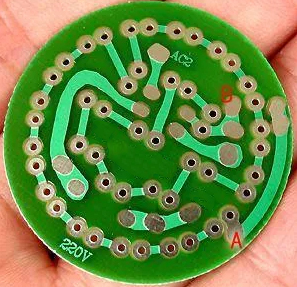
3. Island Pad--It is the integration of the connection between the pad and the pad. It is often used in vertical irregular arrangement installation.
4. Polygonal Pad--It is used to distinguish pads with close outer diameters but different apertures, which is convenient for processing and assembly.
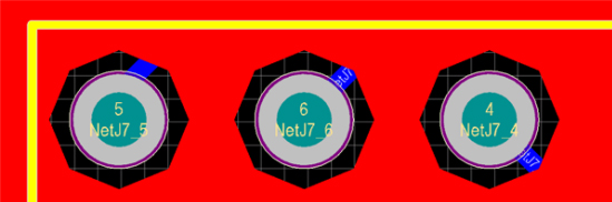
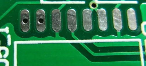
5. Oval Pad--This kind of pad has enough area to enhance the anti-stripping ability, and is often used in dual in-line devices.
6. Open Pad--In order to ensure that after wave soldering, it is often used when the manually repaired welding pad hole is not sealed by solder.
Ⅱ. Special Pad
1. Plum Blossom Pad
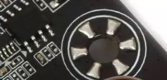
Torx pads are usually used for grounding locations of large vias. There are several reasons for this design:
1) The fixing hole needs to be metalized and connected to GND. If the fixing hole is fully metalized, it is easy to block the hole during reflow soldering process.
The use of internal metal screw holes may result in poor grounding due to installation or multiple disassembly and assembly. However, no matter how the pressure changes, the use of plum blossom pads can ensure good grounding.
2. Cross Flower Pad
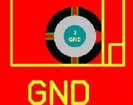
Cross flower pads are also called thermal pads, hot air pads, etc. Its function is to reduce the heat dissipation of the pad during soldering, so as to prevent false soldering or PCB peeling caused by excessive heat dissipation.
1. When your pad is ground. The cross pattern can reduce the area of the ground wire, slow down the heat dissipation speed, and facilitate welding.
When your PCB needs to be assembled with a machine , and it is a reflow soldering machine, because more heat is need to melt the solder paste, the cross pattern pad can prevent PCB peeling.
3. Teardrop Pad
It is often used when the trace connected to the pads are thinner to prevent the pad from peeling off and the traces are disconnected from the pad. Such pads are commonly used in high frequency circuits.


 English
 Français
 Deutsch
 Português
 Pусский
 中文
中文