Welcome to visit Hoyogo website, let's connect the world together!
Customer service hotline:+86 13723413985 or 400 058 2288
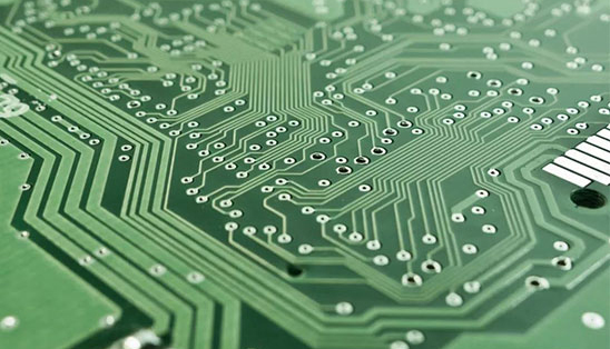
The multilayer PCB design steps are basically the same as the ordinary PCB design steps. The difference is that the routing of the intermediate signal layer and the division of the inner electrical layer need to be divided. It is basically divided into the following steps:
1. Circuit board planning. Mainly to plan the physical size of the PCB, the structure of the board, the packaging form and the installation method of the components.
2. Working parameter settings. Mainly refers to the parameter setting of the working environment and working layer. Setting the PCB environmental parameters correctly and reasonably can improve the work efficiency of PCB design.
3.Component layout and adjustment. After the current work is ready, the net list can be introduced into the PCB, or the net list can be directly introduced in the schematic diagram by updating the PCB. Component layout and adjustment are relatively important tasks in PCB design, which directly affect operations such as the subsequent routing and the division of internal electrical layers.
4. Definition and setting of PCB middle layer. The focus of this operation is to set up a specific layer structure in the software layer stack manager, mainly setting the number of intermediate signal layers and internal electrical layers, upper and lower structures, etc.
5. The inner electric layer segmentation. Usually, the internal power layer often has more than one power supply network. It is often necessary to divide the internal power supply layer into several isolated areas, and connect each area to a specific power supply network. This is the biggest difference between multi-layer boards and ordinary boards, and it is also an important link in multi-layer PCB design. The structure of the internal electrical layer division affects the routing of the power and ground grids, and is also affected by the component layout and routing.
6. Wiring rule setting. Mainly set various specifications of circuit wiring, wire width, parallel wire spacing, safety spacing between wires and pads, and size of vias, etc. No matter which wiring method is adopted, wiring rules are an indispensable step. Good routing rules can ensure the safety of PCB wiring and meet the manufacturing process requirements.
7. Routing and adjustment. In practical applications, designers mainly use automatic routing combined with manual interactive routing to complete the routing work. Special attention should be paid to the characteristics of layout and routing as well as the PCB has the feature of an internal electrical layers. Although the layout and wiring are in order, in the design project, the layout of the PCB will be adjusted according to the needs of wiring and internal electrical layer division, or the wiring will be adjusted according to the layout. They are a process of mutual consideration and mutual adjustment.
8. Other auxiliary operations. For example, operations such as copper coating and teardrop filling, as well as document processing work such as report output and save printing. These files can be used to check and modify PCBs, and can also be used as a list of purchased components.
SHENZHEN HOYOGO ELECTRONIC TECHNOLOGY CO., LTD. has a PCB design team with more than 12 years of work experience. We are not only proficient in using mainstream PCB design software in the market, but also can conduct professional and efficient communication to ensure the progress of PCB design.


 English
 Français
 Deutsch
 Português
 Pусский
 中文
中文