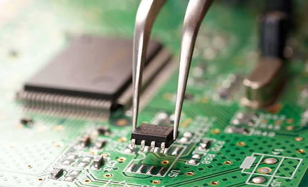
In the circuit board manufacturing process, from technological review to production to final inspection, many aspects of technological work are involved, and the monitoring and control of technological quality and production quality must be considered.

I. Technological Review
Technological review is based on the original materials provided by the design, in accordance with the relevant "PCB design specifications" and related standards, combined with the actual production, to conduct a process review of the relevant design materials for manufacturing circuit boards provided on the design site. The main points of the technological review are as follows:
1. Whether the design data is complete (including: floppy disk, technical standards for implementation, etc.)
2. Bring up the floppy disk data and conduct a technological inspection, which should include circuit patterns, solder mask patterns, drilling patterns, digital patterns, electrical measurement patterns and related design data, etc.;
3. Whether the technological requirements are feasible, manufacturable, electrically testable, maintainable, etc.
II. Technological Preparation
It refers to the technological preparation before production based on the relevant technical data design. The techniques should be scientifically compiled in accordance with the technology procedure, and its main content should include the following aspects:
1. In formulating technology procedures, they must be reasonable, accurate, easy to understand and feasible;
2. In the first process, the front and back sides, welding surfaces and component surfaces of the negatives should be indicated, and numbered or marked;
3. In the drilling process, the aperture type, aperture size and aperture quantity shall be indicated;
4. When making holes, the technical requirements for the copper immersion layer and the backlight detection or measurement shall be indicated;
5. When electroplating after drilling, the initial current size and the technological method of returning to the original normal current size should be indicated;
6. When the pattern is transferred, it is necessary to indicate the correct contact between the film surface of the negative film and the photoresist film and the test conditions of the exposure conditions are determined, and then perform the exposure;
7. The semi-finished product after exposure should be placed for a certain period of time before it can be developed.
8. When pattern plating is thickened, the exposed copper parts should be cleaned and inspected strictly; and check the thickness of copper plating and other technological parameters, such as current density, bath temperature, etc.;
9. When electroplating anticorrosive metal tin-lead alloy, the thickness of the cladding should be indicated;
10. The first test should be carried out during the etching process. After confirming the conditions, perform the etching. After etching, the neutralization treatment must be carried out.
11. In the process of multi-layer board production, pay attention to the inspection of the inner layer graphics or AOI inspection, and then transfer to the next process after passing;
12. When laminating, the technological conditions shall be indicated;
13. If there is a plug gold plating requirement, the plating thickness and plating position shall be indicated;
14. When performing hot air leveling, the process parameters and the matters needing attention when removing the coating should be noted;
15. When molding, the technological requirements and size requirements should be indicated;
16. In the key process, it is necessary to clarify the inspection items, electrical measurement methods and technical requirements.
SHENZHEN HOYOGO ELECTRONIC TECHNOLOGY CO., LTD. is an international, professional, reliable PCB manufacturer. We have 2 production bases with a monthly production capacity of 500,000 square meters. One-stop PCB product supply and solution. And HOYOGO have a management team with 25 years of average industry experience and reliable quality assurance.