Welcome to visit Hoyogo website, let's connect the world together!
Customer service hotline:+86 13723413985 or 400 058 2288
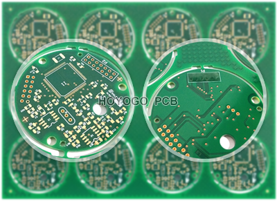
Copper is used to interconnect components on the substrate. Although it is a good conductor material for patterning the conductive path of a printed circuit board, if exposed to the air for a long time, it will easily lose gloss due to oxidation, suffer corrosion and lose its solderability. Therefore, various technologies must be used to protect copper traces, vias, and plated through holes. These technologies include organic paint, oxide film, and electroplating.
Organic paint is very simple to apply, but due to changes in its concentration, composition and curing cycle, it is not suitable for long-term use. It will even cause unpredictable deviations in weldability. The oxide film can protect the circuit from corrosion, but cannot maintain solderability.
Electroplating or metal etching technologies are standard operations to ensure solderability and protect circuits from corrosion, and play an important role in the manufacture of single-sided, double-sided and multilayer printed circuit boards. In particular, plating a layer of weldable metal on the printed wire has become a standard operation for the copper printed wire to provide a weldable protective layer.
In electronic equipment, the interconnection of various modules usually requires the use of a printed circuit board socket with spring contacts and a printed circuit board with matching connection contacts. In electronic equipment, the interconnection of various modules usually requires the use of a printed circuit board socket with spring contacts and a printed circuit board with matching connection contacts. These contacts should have a high degree of wear resistance and very low contact resistance, which requires a layer of rare metal plating on them. The most commonly used metal is gold. In addition, other coated metals can be used on printed circuits, such as tin plating, silver plating, and sometimes copper plating in certain printed areas.
Another type of coating on the copper printed line is organic, usually a solder mask. Use screen printing technology to cover a layer of epoxy resin film where welding is not required. This technology of applying a layer of organic solder protection agent does not require electronic exchange. When the circuit board is immersed in the electroless plating solution, a nitrogen-resistant compound can stand on the exposed metal surface and will not be absorbed by the substrate.
The precise technology required by electronic products and the strict requirements of environmental and safety adaptability have promoted considerable progress in electroplating practice. In electroplating, through the development of automated, computer-controlled electroplating equipment, the development of highly complex instrumentation technology for chemical analysis of organics and metal additives. As well as the emergence of technologies that precisely control the chemical reaction process, electroplating technology has reached a very high level.
There are 2 standard methods for growing metal build-up layers in circuit board wires and vias as follows:
1. Circuit Plating
In this process, the copper layer and the metal plating layer of resist can only be produced where the circuit patterns and through holes are designed. During the circuit electroplating process, the increased width of each side of the circuit and the solder pad is approximately equal to the increased thickness of the electroplated surface. So, it is necessary to leave a margin on the original film.
In circuit electroplating, most of the copper surface must be masked by resist, and electroplating is performed only where there are circuit patterns such as circuits and solder pads. As the surface area that needs to be plated decreases, the required power supply current capacity is usually greatly reduced. In addition, when using contrast reversal photosensitive polymer dry film electroplating resist, relatively inexpensive laser printers or drawing pens can be used to make negatives. The copper consumption of the anode in the line electroplating is reduced, and the copper that needs to be removed during the etching process is also reduced, thus reducing the analysis and maintenance costs of the electrolytic cell. The disadvantage of this technique is that the circuit pattern needs to be plated with tin/lead or an electrophoretic retarder material before etching, and it is removed before applying the solder resist. This adds complexity and an additional set of wet chemical solution treatment processes.
2. Full Board Copper Plating
In this process, all surface areas and drill holes are plated with copper, and then some resist is injected on the unwanted copper surface, and then plated with corrosion-resistant metal. Even for medium-sized printed circuit boards, this requires an electric excavator that can provide a large amount of current to form a smooth and bright copper surface that is easy to clean and can be used in subsequent processes. If you don't have an optoelectronic plotter, you need to use a negative film to expose the circuit pattern, which makes it a more common contrast inversion dry film photoresist.
HoYoGo can offer FR4 1-56 Layer, HDI, gold finger, hard gold, flexible PCB, rigid-flex PCB, metal base PCB, quick-turn and PCBA. The base material also depends on the requirement, it can be KB, SY, NY, ITEQ, etc.


 English
 Français
 Deutsch
 Português
 Pусский
 中文
中文