Welcome to visit Hoyogo website, let's connect the world together!
Customer service hotline:+86 13723413985 or 400 058 2288
Copper deposition is an important part of PCB design. No matter what kind of PCB design software provides smart Copper clad function. So how to clad copper?
In fact, the so-called copper is to use the free space on the PCB as a reference plane, and then fill it with solid copper. These copper areas are also referred to as copper fills. The significance of copper plating is to reduce the impedance of the ground wire and improve the anti-interference ability. Reduce voltage drop and improve power efficiency; connecting to ground wire can also reduce loop area. In order to keep the PCB from deforming as much as possible, most PCB manufacturers will also require PCB designers to fill the copper area or grid-like ground wire in the open area of the PCB. If PCB has more grounding, such as SGND, AGND, GND, etc., how to clad copper? According to the different positions of PCB surface, we use the most important "ground" as the reference to clad copper independently, and separate digital ground and analog ground to clad copper. At the same time, before copper plating, we must first thicken the corresponding power connections: v5.0v, v3.6v, v3.3v, etc. In this way, multiple deformable structures with different shapes can be formed.
There are several issues that need to be dealt with in copper clad: The first is the single point connection of different grounds, the method is to connect through 0 ohm resistance or magnetic beads or inductance. The second is the copper coating near the crystal oscillator. The crystal oscillator in the circuit is a high-frequency emission source. The method is to clad copper around the crystal oscillator, and then ground the crystal oscillator shell separately. The third is the problem of isolated islands (dead zones). If you feel the area is large, it is not important to add a ground via.
In addition, whether large area copper is good or grid copper is good, not easy to generalize. why? Large area copper clad, if wave soldering, the circuit board may warp or even blisters. From this point of view, the cooling effect of the grid is better. It is usually a multi-purpose power grid, which has high requirements for anti-interference of high-frequency circuits and the low frequency circuit is accompanied by circuits with large currents and other commonly used complete copper laying.
Summary: When you start wiring, you should treat the ground wire equally. When routing, you should route the ground wire well. You cannot rely on adding copper vias to eliminate the ground pin connected. This effect is very bad. Of course, if you choose grid copper, these grounds will affect the appearance. In short: the copper clad on the PCB, if the grounding problem is solved, it must be "benefits outweigh the disadvantages". It can reduce the return area of the signal line and reduce the electromagnetic interference of the signal to the outside.
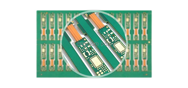
HOYOGO is an international, professional, reliable PCB manufacturer. We have 2 production bases with a monthly production capacity of 500,000 square meters. One-stop PCB product supply and solution. And HOYOGO have a management team with 25 years of average industry experience and reliable quality assurance.


 English
 Français
 Deutsch
 Português
 Pусский
 中文
中文