Welcome to visit Hoyogo website, let's connect the world together!
Customer service hotline:+86 13723413985 or 400 058 2288
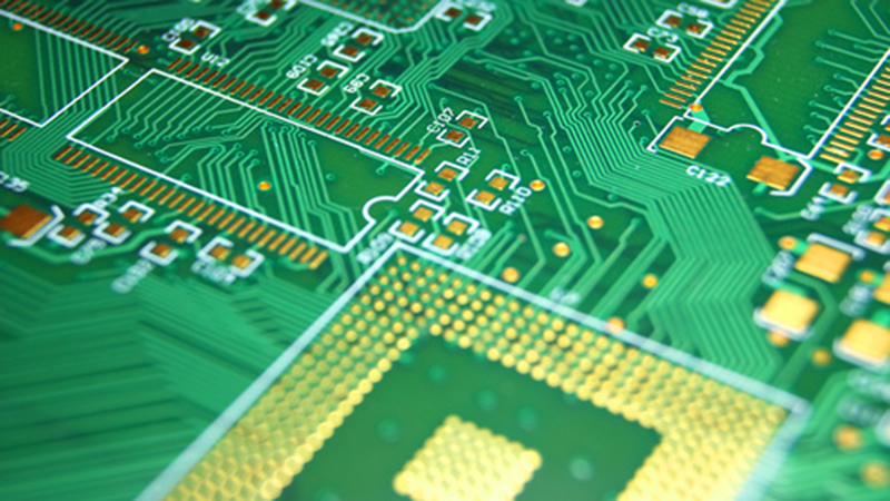
PCB routing is to lay out printed wires according to the PCB circuit schematic diagram, wire table, and the required wire width and spacing. The routing should generally comply with the following rules:
1. The PCB routing should be as simple as possible on the premise of meeting the requirements of use. The order of selecting the routing method is single layer - double layer - multilayer.
2. The wire layout between the two patch connection plates should be as short as possible, and sensitive signals and small signals should go first to reduce the delay and interference of small signals. Ground shielding should be designed near the input line of the analog circuit; the wiring of the same layer should be evenly distributed; the conductive area on each layer should be relatively balanced to prevent PCB warping during processing.
3. When changing the direction of the signal line, a diagonal or smooth transition should be taken, and the radius of curvature should be larger to avoid electric field concentration, signal reflection and additional impedance.
4. Digital circuits and analog circuits should be separated in wiring to avoid mutual interference. If they are on the same layer, the wires of the ground system and the power supply system of the two circuits should be laid separately, and the signal wires of different frequencies should be separated by laying ground wires to avoid crosstalk. If they are on the same layer, the wiring of the grounding system and the power supply system of the two circuits should be separated, and the signal wires of different frequencies should be separated by laying ground wires to avoid crosstalk. In order to facilitate testing, necessary breakpoints and test points should be set in the design.
5. When circuit components are grounded and connected to power, the traces should be as short and as close as possible to reduce internal resistance.
6. The upper and lower layer traces should be perpendicular to each other to reduce coupling, and the upper and lower traces should not be aligned or parallel. Reasonable wiring layout in PCB patch processing can reduce the defect rate of products.
7. The lengths of multiple I/O lines of high-speed circuits and I/O lines of circuits such as differential amplifiers and balanced amplifiers should be equal to avoid unnecessary delay or phase shift.
8. When the PCB pad is connected to a conductive area with a larger area, a thin wire with a length of not less than 0.5m should be used for thermal isolation, and the width of the thin wire should not be less than 0.13mm.
9. The wire closest to the edge of the SMB should be more than 5mm away from the edge of the SMB. If necessary, the ground wire can be close to the edge of the SMB. To insert the guide rail during SMT processing, the distance between the wire and the edge of the SMB must be at least greater than the depth of the guide groove.
10. The common power lines and ground lines on the double-sided SMB should be routed as close to the edge of the SMB as possible, and distributed on both sides of the SMB. The multi-layer SMB can be provided with a power supply layer and a ground line layer on the inner layer, and is connected to the power line and ground line of each layer through metallized holes. The large-area wires, power wires and ground wires of the inner layer should be designed into a net shape, which can improve the bonding force between the multi-layer SMB layers.
SHENZHEN HOYOGO ELECTRONIC TECHNOLOGY CO., LTD. has a PCB design team with more than 12 years of work experience. We are not only proficient in using mainstream PCB design software in the market, but also can conduct professional and efficient communication to ensure the progress of PCB design. We are a professional PCB design company that can help customers in related industries seize market opportunities as early as possible.


 English
 Français
 Deutsch
 Português
 Pусский
 中文
中文