Welcome to visit Hoyogo website, let's connect the world together!
Customer service hotline:+86 13723413985 or 400 058 2288
PCB plays an extremely important role in electronic products, and it is the core part of electronic products. PCB has grown from single-layer to double-sided boards, multilayer boards and flexible boards, and continues to develop towards high precision, high density and high reliability. By continuously reducing the size, reducing costs, and improving performance, printed circuit boards will still maintain a strong vitality in the future growth of electronic products.
1. Manufacturability: With modern management, standardized, scoped and automated production can be carried out to ensure equal product quality.
2. High-density: For decades, with the improvement of integrated circuit integration and placement technology, high-density printed circuit boards can be developed.
3. High-reliability: Through a series of inspection, testing and aging test, the permanence and reliability of the PCB can be guaranteed. The service life of PCB is usually 20 years.
4. Testability: A relatively complete test method, test standard, various test setup equipment deployment and instruments have been created to detect and determine the qualification and service life of PCB products for PCB proofing.
5. Planability: For the various properties of PCB, such as electrical, physical, chemical, mechanical, etc., the printed circuit board plan can be realized through plan standardization and paradigmization.
6. Assemblability: PCB products not only contribute to the standard assembly of various components, but also contribute to automation and mass production. At the same time, PCB and various component assembly parts can be assembled to form larger parts and systems, up to the complete machine.
7. Maintainability: With the standardization and mass production of PCB products and various assembly parts, these parts have also been standardized. Once the system is obstructed, it can be replaced quickly, conveniently and flexibly to quickly restore the system. Of course, there are also more examples. Such as system miniaturization and light weight, and high-speed signal transmission.
The PCB circuit board is mainly composed of pads, vias, mounting holes, wires, components, connectors, filling, electrical boundaries, etc. The main functions of each component are as follows:
Pad: It is used as a metal hole for welding component pins.
Via: It is used to connect the metal holes of the component plugs between the layers.
Mounting Hole: It is used as a fixed printed circuit board.
Wire: It is used to connect the electrical grid copper film of the component pins.
Connector: It is used for components connected between circuit boards.
Filling: It is used for the copper coating of the ground grid, which can effectively reduce the impedance.
Electrical Boundary: It is used to determine the size of the circuit board, and all components on the circuit board cannot exceed the boundary.
Common layer structures of PCB circuit boards include single layer PCB, double layer PCB and multiple PCB. The brief description of these three layer structure is as follows:
1. Single layer PCB: That is, a circuit board with copper on one side and no copper on the other side. The components are usually placed on the side without copper, and the side with copper is mainly used for wiring and soldering.
2. Double layer PCB: That is, a circuit board with copper on both sides, usually called the top layer on one side and the bottom layer on the other side. Generally, the top layer is used as the component placement surface, and the bottom layer is used as the component welding surface.
3. Multilayer PCB: That is, in addition to the top and bottom layers, a circuit board that also includes multiple working layers also includes multiple intermediate layers. Generally, the middle layer can be used as a wire layer, signal layer, power layer, ground layer, etc. The layers are insulated from each other, and connections between the layers are usually achieved through vias.
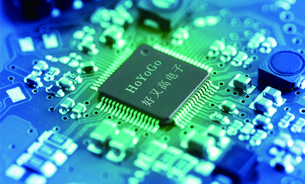
SHENZHEN HOYOGO ELECTRONIC TECHNOLOGY CO., LTD. is a manufacturer specializing in the production of high-precision double-sided, multilayer and impedance, blind buried vias, thick copper circuit boards. The products cover various circuit boards such as HDI, thick copper, backboard, rigid-flex combination, embedded capacitors, gold fingers, etc., which can meet the needs of customers for various products.


 English
 Français
 Deutsch
 Português
 Pусский
 中文
中文