Welcome to visit Hoyogo website, let's connect the world together!
Customer service hotline:+86 13723413985 or 400 058 2288
SHENZHEN HOYOGO ELECTRONIC TECHNOLOGY CO., LTD. has a PCB design team with more than 12 years of work experience. We are not only proficient in using mainstream PCB design software in the market, but also can conduct professional and efficient communication to ensure the progress of PCB design. We are a professional PCB design company that can help customers in related industries seize market opportunities as early as possible.
An excellent PCB design engineer needs to master a wide range of knowledge systems, which should cover electrical theory, component performance, digital and analog circuits, PCBA processing technology and DFM manufacturability theory, soldering practice operations, schematic drawing and layout, single-chip microcomputer Program logic and basic principles, etc.
1. If the design circuit system contains FPGA devices, you must use the Quartus II software to verify the pin assignments before drawing the schematic, because some special pins in the FPGA cannot be used as ordinary IO.
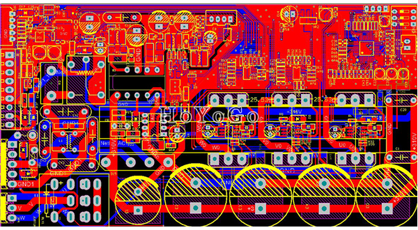
2. The structure of the 4-layer board from top to bottom is: signal plane layer, ground layer, power supply layer, signal plane layer;
The structure of the 6-layer board from top to bottom is: signal plane layer, ground layer, signal inner electric layer, signal inner electric layer, power supply layer, signal plane layer.
Advantages of 6-layer boards or more: It can prevent interference radiation.
Disadvantages of 6-layer boards or more: It will divide the power layer and produce parasitic effects.
Improvement method: The inner electric layer wiring should be selected first. If the wiring cannot be successfully routed after this selection, re-select the wiring from the plane layer, and absolutely prohibit routing from the ground or power layer.
3. Multi-power supply system wiring: If the FPGA + DSP system consists of 6-layer boards, there will be at least 3.3V + 1.2V + 1.8V + 5V.
3.3V is generally the main power supply, and the power layer is directly laid, and the global power network is easily wired through the vias;
5V may generally be the power input, and only a small area need to be coppered. And the copper is as thick as possible.
1.2V and 1.8V are the core power supply. If it directly uses wire connection, it will encounter great difficulties when facing BGA devices.
Please separate 1.2V and 1.8V as much as possible during layout, and arrange the components connected within 1.2V or 1.8V in a compact area, and use copper sheet to connect.
In short, because the power supply network is spread over the entire PCB, it will be very complicated and long to go around if you use the wiring method, so the method of laying copper is a good choice!
4. The wiring between adjacent layers adopts a cross method: it can reduce electromagnetic interference between parallel wires and facilitate wiring.
5. Analog and digital must be isolated, how to isolate it?
During layout, the components used for analog signals should be separated from those used for digital signals, and then cut across the AD chip!
The analog signal is laid with an analog ground, and the analog ground/analog power supply and the digital power supply are connected at a single point through an inductor/magnetic bead.
6. PCB design based on PCB design software can also be regarded as a software development process. Software engineering pays most attention to the idea of "iterative development" to reduce the probability of PCB errors.
(1) When checking the schematic diagram, please pay attention to the power and ground of the device, because the power and ground are the blood of the system, and there can be no negligence;
(2) When drawing the PCB package, please confirm whether the pins in the schematic diagram are wrong;
(3) After confirming the PCB package size one by one, please add a verification label to the package library of this design;
(4) When importing the netlist, please adjust the signal sequence in the schematic while laying out. After layout, the automatic component numbering function of OrCAD can no longer be used.


 English
 Français
 Deutsch
 Português
 Pусский
 中文
中文