Welcome to visit Hoyogo website, let's connect the world together!
Customer service hotline:+86 13723413985 or 400 058 2288
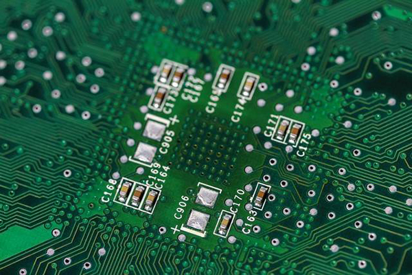
PCB pulse plating not only significantly improved the quality and in productivity efficient of common multilayer board, but also an indispensable and important method in blind via plating of high aspect ratio multilayer boards and HDI multilayer boards. Do you know why?
1. Pulse plating can better solve the problem of uniformity of copper plating thickness in PCB holes, and make the thickness of copper plating in PCB holes close to the thickness of copper plating on the board surface. In other words, the difference between the thickness of the copper plating on the board surface and the hole is reduced, and the gradient problem of the thickness of the copper plating from the hole to the middle of the hole is improved. Therefore, the quality and reliability of the connection in the PCB hole are improved, which is conducive to the conditions for manufacturing fine wires on the board surface.
2. For high aspect ratios (5:1~20:1), micro holes and blind vias, it is difficult for traditional DC plating to solve the disparity between the thickness of the copper layer in the hole and thickness of the copper layer on the board surface, while pulse plating can solve this problem better.
3. Because the thickness of the copper plating layer on the board is much smaller than the thickness of the copper plating layer on the board obtained by DC plating. Therefore, it is very conducive to etching fine wires and can improve the PCB production qualification rate for characteristic impedance value control.
4. Pulse plating can use greater current densities by more 30%. The duration of the plating technology is shortened, so at the same scale, pulse current plating can increase productivity by 50% compared to DC plating.
5. The cost savings when using pulse current plating are mainly reflected in: Solder mask ink consumption, anode copper balls and increased productivity. Therefore, the cost savings can be calculated based on the production volume.
HoYoGo is an international, professional and reliable PCB factory, we are committed to providing customers with stable quality, professional PCB manufacturing and PCB assembly services. We have more than 12 years of PCB production experience. If you have related needs, you are welcome to send us an inquiry.


 English
 Français
 Deutsch
 Português
 Pусский
 中文
中文