Welcome to visit Hoyogo website, let's connect the world together!
Customer service hotline:+86 13723413985 or 400 058 2288
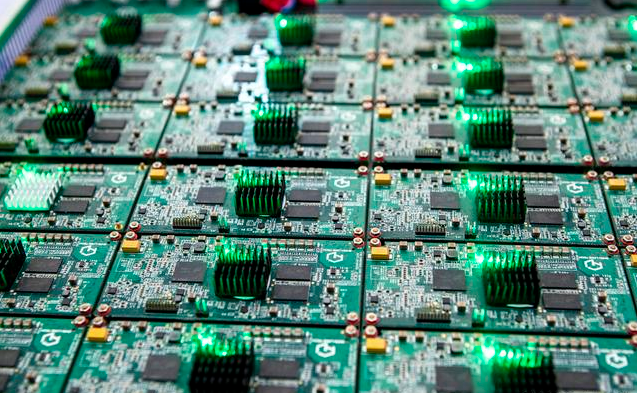
Nowadays, PCB wave soldering has become the most commonly used process method for soldering circuit board. This method is suitable for soldering printed circuit boards with discrete components and integrated circuits on one side in batches and in large quantities. So what are the advantages of PCB wave soldering?
Working Principle:
Wave soldering uses a mechanical or electromagnetic centrifugal pump in the solder bath to press the molten solder to the nozzle, forming a smooth upward wave of solder and continuously overflowing from the nozzle. The printed circuit board equipped with components moves through the wave soldering in a plane and straight line at a uniform speed, forming infiltrated solder joints on the soldering surface to complete the soldering.
Advantages:
1. A layer of antioxidants floats on the surface of the molten solder to isolate the air. As long as the wave soldering is exposed to the air and the chance of oxidation is reduced, the solder waste caused by oxide slag can be reduced.
2. The circuit board is exposed to high-temperature solder for a short time, which can reduce the warping deformation of the circuit board.
3. The solder in the dip soldering machine is relatively static, and the metals with different densities in the solder will produce delamination. Under the action of the solder pump, the wave soldering machine circulates the molten solder in the whole tank to make the solder composition uniform.
4. The solder of the wave soldering machine is fully flowing, which is conducive to improving the quality of solder joints.
In addition, some questions should be paid attention to in the wave soldering process, for example: Before wave soldering, please check the operation of the equipment, the quality of the PCB to be soldered and the condition of the DIP.
SHENZHEN HOYOGO ELECTRONIC TECHNOLOGY CO., LTD. is a company specializing in providing overall PCBA electronic manufacturing services, including one-stop services from upstream electronic components procurement to PCB production and processing, SMT placement, DIP, PCBA testing, and finished product assembly.


 English
 Français
 Deutsch
 Português
 Pусский
 中文
中文