Welcome to visit Hoyogo website, let's connect the world together!
Customer service hotline:+86 13723413985 or 400 058 2288
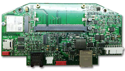
If the PCB does not meet the requirements, it will increase the difficulty of the PCBA soldering process, which may eventually lead to soldering defects or unqualified PCBA. So, in order to ensure the efficient completion of PCBA processing, the PCB should meet the following requirements as much as possible:
1. PCB Size
The ideal size of PCB (including board edge) is - width≧50mm, <460mm, length≧50mm. If the size of the design is too small, a panel includes 2 different kinds of PCB needs to be made.
2. PCB board edge width
The board edge width of the PCB needs to be >5mm, the panel includes 2 different kinds of PCB spacing <8mm, and the distance between the pad and the board edge is >5mm.
3. PCB bending
The warpage of the PCB board will affect the placement accuracy and will cause the PCB to move unevenly in the direction of the conveyor belt, so the warpage of the PCB board should be as small as possible. The requirements for bending degree are - upward bending degree: <1.2mm, downward bending degree: <0.5mm, PCB distortion: maximum deformation height ÷ diagonal length <0.25.
4. Mark point of PCB board
In the actual PCBA processing, we need to pay attention to many problems in the setting of Mark point of the board, and it is also more important. The size of Mark is generally in the range of 0.8~1.5mm. Its surface needs to be flat, smooth, free of oxidation and pollution. There should be no green oil or other obstacles within 1mm around the mark point, and the color should be obviously different. Its position needs to be more than 3mm away from the edge of the board, and there can be no Mark-like vias, test points, etc. within 5mm of it.
5. PCB pad
There must be no through holes on the pads of SMD components. If there is a through hole, the solder paste will flow into the hole, which will cause the device to lose tin or the tin flows to the other side, causing the board surface to be uneven and unable to print the solder paste.
The above are some of the requirements of PCBA processing for PCBs. Every link in the production of PCBs is required to be in place. Only by producing high-quality and qualified PCB can it better accept other special processes.
SHENZHEN HOYOGO ELECTRONIC TECHNOLOGY CO., LTD. specializes in providing overall PCBA electronics manufacturing services, including one-stop services from upstream electronic component procurement to PCB production and processing, SMT patch, DIP plug-in, PCBA testing and finished product assembly.


 English
 Français
 Deutsch
 Português
 Pусский
 中文
中文