Welcome to visit Hoyogo website, let's connect the world together!
Customer service hotline:+86 13723413985 or 400 058 2288
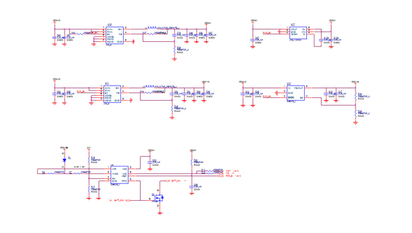
The circuit board design scheme is based on the circuit schematic diagram to realize the functions required by the circuit designer. The PCB circuit board design scheme mainly refers to the layout design, which needs to consider various factors, such as the layout of external connections, the optimized layout of internal electronic components, the optimized layout of metal connections and through holes, electromagnetic protection and heat dissipation, etc. Excellent layout design can save production costs and achieve good circuit performance and heat dissipation performance. Simple layout design can be realized by hand, while complex layout design needs to be realized by computer-aided design.
In high-speed design, the characteristic impedance of the controllable impedance board and circuit is one of the most important and common problems. First understand the definition of a transmission line: a transmission line is composed of two conductors with a certain length, one conductor is used to send signals, and the other is used to receive signals (please be sure to remember the concept of "loop" instead of "ground"). In a multilayer board, each line is a component of the transmission line, and the adjacent reference plane can be used as the second line or loop. The key to making a line a "good performance" transmission line is to keep its characteristic impedance constant throughout the line.
The key for a circuit board to become a "controllable impedance board" is to make the characteristic impedance of all lines meet a specified value, usually between 25 ohms and 70 ohms. In multilayer circuit boards, the key to obtaining good transmission line performance is to keep its characteristic impedance constant throughout the circuit.
But what is the characteristic impedance? The easiest way to understand characteristic impedance is to see what the signal encounters during transmission. When moving along a transmission line with the same cross-section, such as connecting a 1 volt battery to the front end of the transmission line (it is located between the transmission line and the loop). Once connected, this voltage wave signal propagates at the speed of light along this line, and its speed is usually about 6 inches/nanosecond. Of course, this signal is indeed the voltage difference between the transmission circuit and the loop, which can be measured from any point of the transmission circuit and the adjacent point of the loop.
The headquarter address of SHENZHEN HOYOGO ELECTRONIC TECHNOLOGY CO., LTD. is located at the A/7F, Kechuang Building, Quanzhi Science and Technology Innovation Park, Shajing Street, Bao'an District, Shenzhen. 518104/ P.R.C. We have been focusing on electronic product development for a long time, with independent R&D team and rich industry experience. We can also provide customers with high-quality professional hardware development, PCB LAYOUT, and one-stop electronic product ODM services from PCB manufacturing to PCBA and complete machine assembly, and win-win cooperation with customers.


 English
 Français
 Deutsch
 Português
 Pусский
 中文
中文