Welcome to visit Hoyogo website, let's connect the world together!
Customer service hotline:+86 13723413985 or 400 058 2288
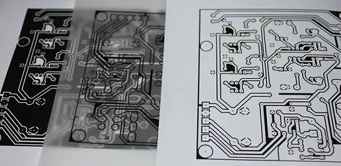
In the PCB production process, it is often necessary to use photoresist film for pattern transfer. There are two types of photoresist film, positive and negative. These two types of photoresist films are very different in use. Do you know the difference between these two technologies?
1. The difference between film circuit diagram
The circuit or copper surface required for the positive is black or brown, and the unnecessary parts are transparent. A negative is the opposite of a positive. The desired circuits or copper surfaces are transparent, while the unwanted parts are black or brown.
The light-shielding and light-transmitting parts of the positive and negative circuit are opposite. The positive needs to be tinned and protected after removing the uncured film to expose the copper surface, and then dissolve it with alkaline solution. Without the copper foil protected by tin and lead, what is left is the circuit we want. The negative directly corrodes the exposed copper surface after removing the uncured film, leaving the circuit protected by the cured dry film.
2. Differences in the production process
Positive is generally graphic processes, and the liquid used is alkaline etching. The positive is copper-free by default, because in the terms of effect presented, copper is retained in the areas where the traces and copper are laid in the positive technology, and there is no copper in the areas where there are no traces and copper laying. The positive technology has more electroplating processes than the negative technology, and the production time is longer than the negative technology.
Negative is generally produced using the tenting process, which uses acidic etching. The negative has copper by default. In terms of presentation effect, there is no copper retained in the areas where the traces and copper are laid in the negative process, while there is copper in the areas where there are no traces and copper laying. During the manufacturing process, the film has to cover the holes, and the requirements for exposure and films are slightly higher, but the manufacturing process is fast.
HoYoGo is an international, professional and reliable PCB manufacturer. The management team has an average of 25 years of industry experience. We also have 2 factory production bases with a monthly production capacity of 500,000 square meters. With our rich experience, production capacity and resources, we can provide you with one-stop service with small, medium to mass production.


 English
 Français
 Deutsch
 Português
 Pусский
 中文
中文