Welcome to visit Hoyogo website, let's connect the world together!
Customer service hotline:+86 13723413985 or 400 058 2288
Generally speaking, the more complex the functions of electronic products, the longer the loop distance, the more contact pins, and the more layers the PCB needs.
The substrate of the circuit board itself is made of an insulating and non-flexible material. The tiny circuit material that can be seen on the surface is copper foil. The copper foil was originally covered on the entire board, but part of it was etched away during the manufacturing process, and the remaining part became reticular fine lines. These wires are called wires or routing and are used to provide circuit connections for components on the PCB.
In order to fix the part on the PCB, we solder its pins directly on the wiring. In the most basic single panel, the parts are concentrated on one side, and the wires are concentrated on the other side. In this way, we need to make holes in the board so that the pins can pass through the board to the other side, thereby soldering the pins of the part to the other side. Because of this, the front and back sides of the PCB are called the part side and the solder side respectively.
If some parts on the PCB need to be removed or put back in place after production is completed, sockets will be used when installing the parts. Since the socket is directly welded on the board, the parts can be disassembled and assembled at will.
If you want to connect two PCBs to each other, we generally use side connectors commonly known as "gold fingers". There are many exposed copper pads on the golden fingers, which are actually part of the PCB wiring. Usually when connecting, we insert the golden finger on one PCB into the appropriate slot on the other PCB. In a computer, the display card, sound card or other similar interface cards are connected to the motherboard by gold fingers.
The green or brown on the PCB is the color of the solder mask. This layer is an insulating protective layer, which can protect the copper wire and prevent the parts from being welded to the wrong place. Another screen printing surface will be printed on the solder mask. Usually words and symbols are printed on this to indicate the position of each part on the board. The screen printing surface is also called the icon surface.
After careful and neat planning, the printed circuit board etches the complex circuit copper wires between the parts on the circuit board to provide the main support for the installation and interconnection of electronic components. It is an indispensable basic part of all electronic products.
Printed circuit boards are flat plates made of non-conductive materials. The board is usually designed with pre-drilled holes for mounting chips and other electronic components. The hole of the component can help the metal path printed on the board to make the electronic connection. After the pins of the electronic components pass through the PCB, conductive metal welding rods are adhered to the PCB to form a circuit.
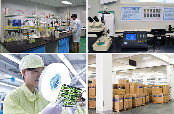
SHENZHEN HOYOGO ELECTRONIC TECHNOLOGY CO., LTD. is an international, professional, reliable PCB manufacturer. We have 2 production bases with a monthly production capacity of 500,000 square meters. One-stop PCB product supply and solution. And HOYOGO have a management team with 25 years of average industry experience and reliable quality assurance.


 English
 Français
 Deutsch
 Português
 Pусский
 中文
中文