Welcome to visit Hoyogo website, let's connect the world together!
Customer service hotline:+86 13723413985 or 400 058 2288
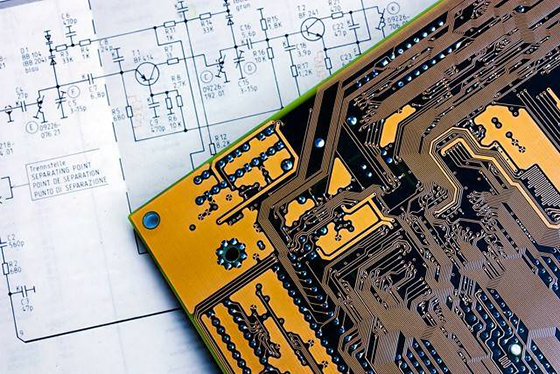
The purpose of the solder mask is to prevent conductor from being stained with tin, prevent short circuits between conductors caused by moisture, chemicals, etc., prevent circuit interruption and insulation caused by poor operation during production and assembly, and resist various harsh environments. It is also used to ensure the functionality of printed circuit board. So do you know what the process of this technology is?
1. Mixing of Solder Mask Inks
The mixing of solder mask ink can be done by manual stirring, mechanical stirring and oscillation. Some solder mask inks need to be added diluent to reduce viscosity. The ink needs to be left for a certain period of time after mixing, usually more than 15 minutes. The purpose is not only to maintain the temperature and viscosity, but also to facilitate the escape of air brought in during stirring.
2. Pretreatment
Pretreatment refers to removing oxides, grease and impurities on the board surface, thoroughly cleaning and roughening the board surface, so that it has good binding force with the solder mask ink.
3. Coating
Coating refers to applying ink to a circuit board. The coating of solder mask ink is mainly based on curtain coating and screen printing.
4. Precure
Precure is to evaporate the solvent in the solder mask ink so that it does not stick to the film when exposed. During the precure process, it should be noted that if the precure is excessive, it will lead to dirty development; if the precure is insufficient, the film will easily stick to the film during exposure, leaving indentations on the film. During development, the solder mask is easily eroded by the developer, causing the surface to lose luster or even the solder mask layer to swell and fall off.
5. Exposure
To put it simply, exposure means that the solder mask ink that needs to remain on the board undergoes a cross-linking reaction after being irradiated with ultraviolet light, and is not removed during development. The non-photosensitive parts are dissolved and washed away by the sodium carbonate solution to expose areas such as connecting pads and welding pads that need to be soldered.
6. Develop
Purpose: The unsensitized part of the ink dissolves in the developer and is washed away, leaving the photosensitive part. During the development process, you need to pay attention: if the concentration of the developer is too high or the temperature is too high, the solder mask layer will be seriously corroded or even expand and fall off.
7. UV Cure
UV cure is to completely cure the remaining photosensitive substances, increase the surface gloss, and help the heat resistance and chemical properties of the solder mask layer.
8. Final Heat Cure
Purpose: To completely cure the solder mask ink, complete a stable mesh structure, and achieve its electrical and physical and chemical properties.
HoYoGo is an international, professional PCB manufacturer. We not only have our own factory, but we also have advanced machines and many years of experience in producing PCB, so we can continue to produce high-quality, high-efficiency products. We have no MOQ and we can even support you with 1 pcs PCB. If you have PCB needs, you are welcome to send us your inquiry.


 English
 Français
 Deutsch
 Português
 Pусский
 中文
中文