Welcome to visit Hoyogo website, let's connect the world together!
Customer service hotline:+86 13723413985 or 400 058 2288
AI vision navigation systems use cameras to capture images of the surrounding environment, combining image processing, AI algorithms, and positioning technologies to support environmental perception and autonomous navigation. These systems are widely used in autonomous mobile robots (AMRs), warehouse logistics robots, and industrial mobile robots. PCBs used in these applications must support high-speed signal transmission, stable electrical performance, and reliable operation in demanding environments. Requirements for image acquisition, data transmission, real-time processing, and operational stability vary depending on the application and hardware platform.
PCBs form an essential part of the electronic hardware in AI vision navigation systems, providing electrical connections, signal transmission, and power distribution between components. They are used in camera modules, AI computing modules, communication interfaces, power management circuits, and control units. As system integration and data processing capabilities increase, these PCBs must accommodate high-density routing while meeting requirements for signal integrity, power integrity, thermal performance, and long-term reliability.
HoYoGo is a professional AI vision navigation system PCB manufacturer specializing in high-reliability, high-precision, multilayer, and high-speed PCBs for intelligent robots, industrial automation, and vision control equipment. To meet the demands of high-speed image transmission, high-density interconnections, and long-term reliability, PCB manufacturing must address circuit fabrication precision, impedance control, multilayer interconnections, power integrity requirements, and manufacturing consistency.
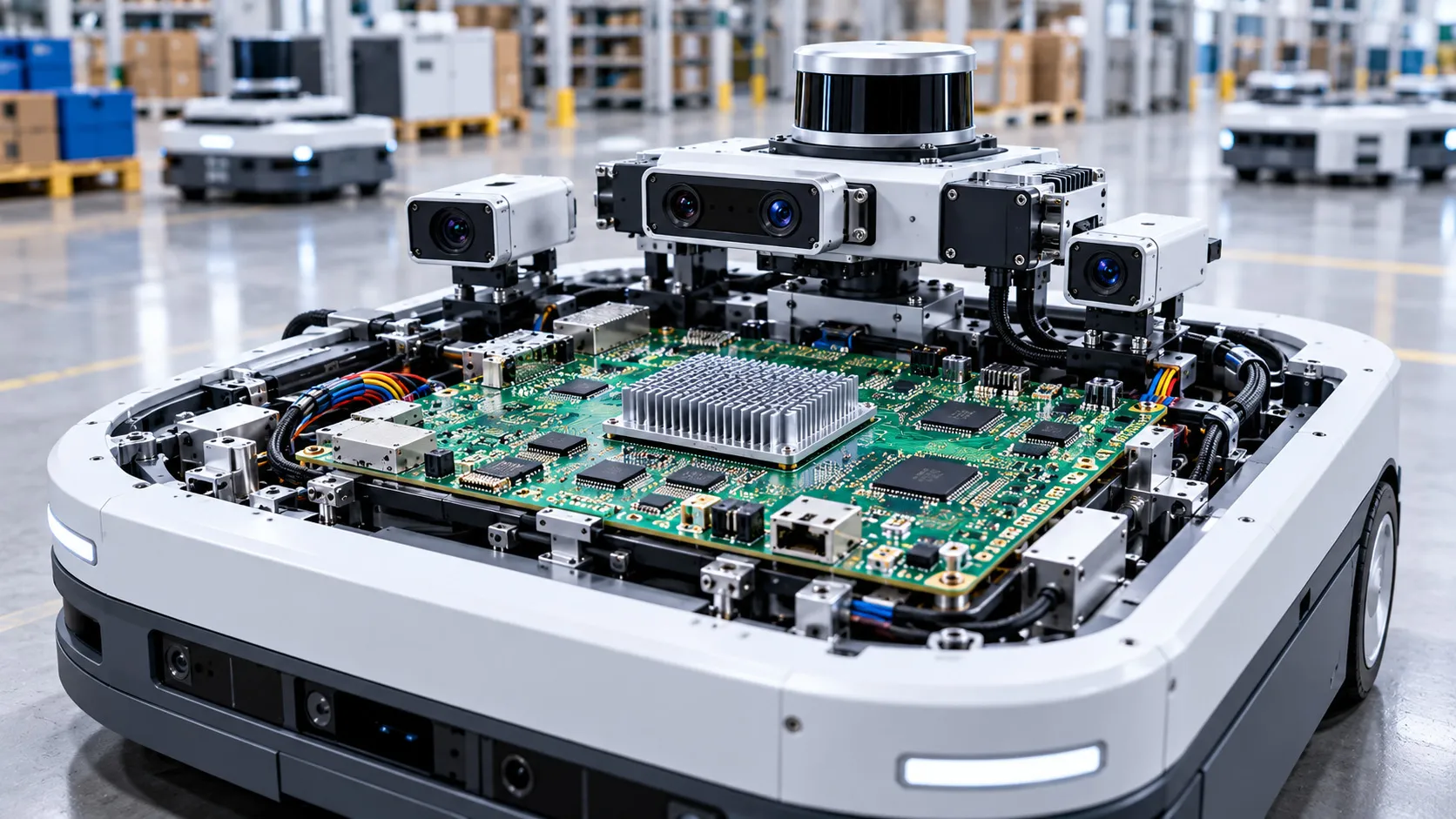
Image Acquisition and High-Speed Signal Transmission
Cameras in AI vision navigation systems transmit captured image data to processors or other relevant computing modules. Some devices use high-speed camera interfaces such as MIPI CSI-2, which place requirements on PCB impedance control, differential pair matching, and signal transmission quality, depending on the interface configuration. Multi-camera systems may incorporate different interface types and connection methods, adding complexity to circuit design and manufacturing.
For controlled-impedance traces, actual impedance is influenced by trace width, copper thickness, dielectric thickness, and material properties. Differential pairs also require appropriate trace spacing. During PCB manufacturing, these parameters must be controlled based on customer-specified stack-up structures, impedance targets, and testing requirements. Impedance testing is then performed under specified conditions to verify that the finished PCBs meet the required electrical specifications.
High-Density Circuits and Multilayer Interconnections
AI vision navigation equipment typically integrates image sensors, processors, memory, and multiple communication interfaces within a compact hardware platform. For robot PCBs with tightly arranged components and high interconnection density, fine-line fabrication, multilayer structures, and precise pad dimensions are important for accommodating dense electrical connections.
Multilayer PCB manufacturing involves several critical processes, including inner-layer circuit fabrication, layer-to-layer registration, lamination, drilling, and hole metallization. The quality of these processes directly affects interconnection reliability. Products incorporating highly integrated processors or high-speed computing modules may require HDI structures, including microvias, to accommodate dense interconnections within limited board space. Manufacturing these PCBs requires precise control of trace dimensions, layer-to-layer registration accuracy, hole positioning, and plated hole quality. Processing methods must also be selected according to the board structure and specified reliability requirements.
Material Selection and Manufacturing Stability
PCBs used in AI vision navigation systems typically carry high-speed image signals, processor interconnections, and power connections. Material performance requirements may differ across functional areas. For high-speed signal traces, dielectric constant (Dk), dissipation factor (Df), and copper foil surface roughness are important factors affecting transmission performance.
Lamination, drilling, and circuit fabrication parameters must be established based on customer-specified materials, technical requirements, and the processing characteristics of the selected laminates. Maintaining material dimensional stability, consistent dielectric thickness, and accurate layer-to-layer registration helps minimize the effects of manufacturing variations on high-speed signal performance and product reliability.
For vision navigation equipment incorporating high-performance processors, thermal management is another important consideration. Appropriate copper layer configurations, heat-conducting structures, and material selection can support heat dissipation and help maintain stable operation over extended periods. These features must be implemented in accordance with the customer's PCB design and technical specifications.
PCB Reliability in Demanding Operating Environments
AI vision navigation equipment is commonly deployed in factories, warehouses, and logistics facilities, where extended operating periods are often required. In autonomous mobile robots and similar equipment, mechanical vibration, temperature fluctuations, and frequent startup and shutdown cycles may affect the long-term reliability of electronic assemblies.
PCB reliability depends on material properties, interlayer bonding quality, plated hole integrity, and surface finishing processes. Temperature variations can introduce thermomechanical stress into PCB materials and interconnection structures, while mechanical vibration may affect board stability and solder joint reliability.
Manufacturing controls must therefore reflect the intended operating environment and customer reliability requirements. Consistent lamination quality, reliable hole-wall copper plating, and effective in-process inspection help reduce the risk of defects such as delamination and barrel cracking.
Manufacturing Consistency in Volume Production
Consistent electronic hardware quality is essential when AI vision navigation equipment enters volume production. For the PCBs used in these systems, variations in trace dimensions, dielectric thickness, copper thickness, via structures, and surface finish quality may affect dimensional accuracy, electrical performance, and consistency between production batches.
Volume PCB manufacturing covers multiple stages, from raw material management and circuit fabrication to lamination, drilling, electroless copper deposition, electroplating, and surface finishing. Each process must follow customer drawings and technical specifications, supported by in-process inspection, final electrical testing, and applicable reliability verification to ensure that every production batch meets the specified manufacturing requirements.
AI vision equipment also incorporates high-speed digital signals, power conversion circuits, and communication modules, making electromagnetic interference (EMI) and electromagnetic compatibility (EMC) important considerations. EMI/EMC performance must be addressed at the system and PCB design stages. During manufacturing, consistent execution of customer-specified stack-up structures, grounding features, and related technical requirements helps maintain the intended electrical characteristics of the PCB.
Development Trends in PCBs for AI Vision Navigation Systems
Multi-camera perception, on-device AI computing, and compact hardware architectures are becoming increasingly common in vision navigation equipment, creating more demanding PCB manufacturing requirements. Camera modules, AI computing boards, and equipment control boards differ in signal types, interconnection methods, and operating environments. Their PCB manufacturing requirements must therefore be evaluated individually.
PCB manufacturers need to establish suitable manufacturing processes based on application conditions, customer design documentation, and reliability requirements. Maintaining stable process control and consistent quality across production batches is essential for supporting the evolving hardware requirements of AI vision navigation equipment.
HoYoGo is a professional AI vision navigation system PCB manufacturer specializing in high-reliability, high-precision, multilayer, and high-speed PCB manufacturing. Based on customer product structures, material specifications, and reliability requirements, we establish appropriate manufacturing processes and carry out production and quality control in accordance with applicable IPC standards and customer technical specifications. We provide reliable PCB manufacturing services for intelligent robots, industrial automation, and AI vision navigation equipment.


 English
 Français
 Deutsch
 Português
 Pусский
 中文
