Welcome to visit Hoyogo website, let's connect the world together!
Customer service hotline:+86 13723413985 or 400 058 2288
As artificial intelligence models grow in scale and computing workloads become more complex, AI servers, GPU accelerator cards, and high-performance computing platforms face increasing demands for data transmission speed, computing density, and operational stability. Processors, high-speed memory, and network interfaces require dense, high-speed signal interconnections, while high-power components place additional demands on power distribution. As a result, high-layer-count PCBs are becoming increasingly common in AI computing equipment.
Compared with conventional multilayer PCBs, high-layer-count PCBs feature more complex stack-ups and interlayer interconnection structures. Material dimensional changes during fabrication and lamination, layer-to-layer registration deviations, and the manufacturing challenges associated with thicker boards and complex hole structures all place stricter demands on fabrication accuracy and product reliability.
HoYoGo is a professional high-layer-count PCB manufacturer specializing in high-precision, high-reliability, and high-speed PCB manufacturing. For AI computing applications, manufacturing these boards requires particular attention to material dimensional stability, layer-to-layer registration accuracy, hole metallization quality, and impedance consistency.
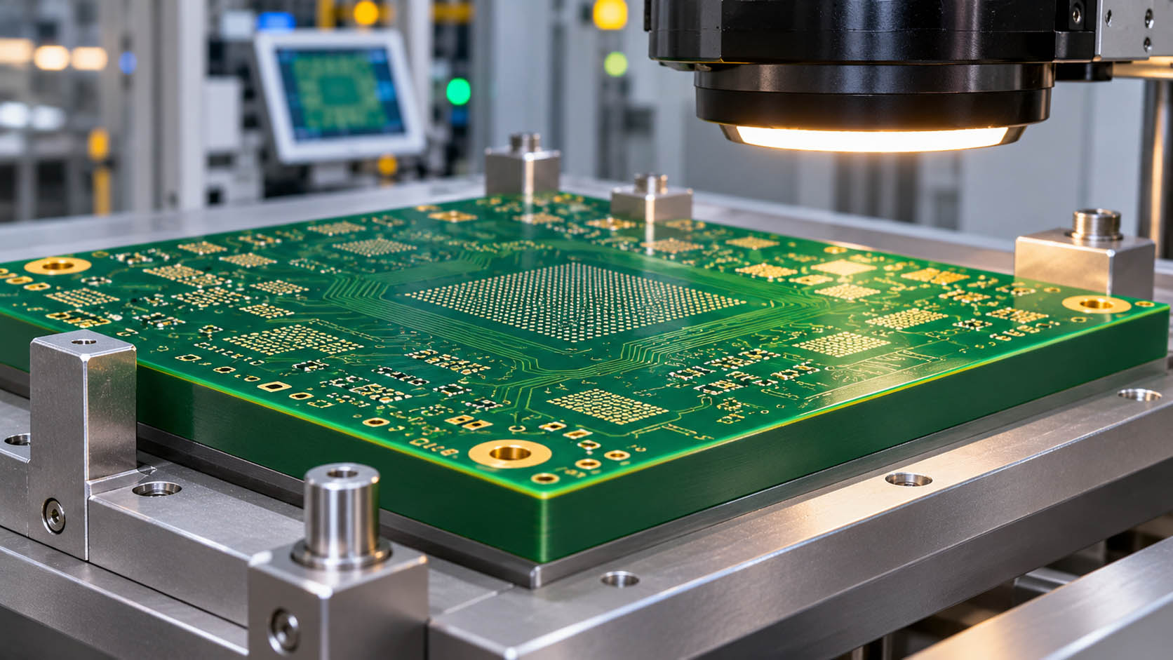
Applications of High-Layer-Count PCBs in AI Computing Equipment
AI servers and high-performance computing systems typically integrate GPUs, CPUs, high-speed memory, and high-speed network interfaces. Their internal electronic systems must accommodate dense signal interconnections and power distribution within limited space. As key electrical interconnection platforms, AI server PCBs must support high-density signal interconnections and ensure reliable power delivery through power traces and planes.
High-layer-count PCBs are used in server motherboards, computing accelerator boards, and certain high-speed interconnect boards. As component integration increases and signal transmission speeds rise, PCBs must provide additional routing layers while accommodating high-speed signal transmission, power distribution, and grounding requirements through appropriate layer structures. Requirements for layer count, circuit fabrication accuracy, material properties, and interlayer connection quality vary across different boards.
For PCB manufacturers, meeting high-layer-count fabrication requirements is only part of the challenge. Inner-layer circuit accuracy and layer-to-layer registration must also be carefully controlled to ensure that circuit structures, interlayer connections, and finished-board electrical performance comply with customer technical specifications.
High-Density Circuitry and Complex Interlayer Interconnections
As the integration density of AI computing equipment continues to increase, some high-layer-count PCBs require finer circuit patterns and more complex interlayer interconnections to accommodate high-density routing within limited space. Controlling trace width, spacing, and via positioning accuracy places greater demands on manufacturing processes.
For PCBs incorporating blind vias, buried vias, and other complex interconnection structures, manufacturers must carefully control via positioning accuracy and interlayer connection quality to meet electrical performance and reliability requirements.
Lamination Processes and Layer-to-Layer Registration Accuracy
High-layer-count PCB manufacturing involves inner-layer circuit fabrication, layer stacking, and lamination. As the number of layers increases, dimensional changes in individual core materials during fabrication and lamination become more difficult to manage, making accurate layer-to-layer registration increasingly challenging.
During lamination, manufacturers must consider material dimensional stability and control temperature, pressure, and processing time according to product requirements. For boards requiring multiple lamination cycles, the effects of repeated thermal processing on material dimensions and interlayer bonding quality must also be considered. Inner-layer copper distribution, material thermal expansion characteristics, and resin flow behavior can further influence dimensional stability and registration accuracy after lamination.
Layer-to-layer registration deviations can cause misalignment between drilled holes and inner-layer pads, potentially compromising the electrical connection between plated hole walls and the corresponding inner-layer pads. Severe misalignment may compromise interconnection reliability. Manufacturers must therefore control inner-layer dimensions and lamination registration accuracy to minimize the effects of fabrication deviations on subsequent drilling and interlayer connections.
High-Aspect-Ratio Drilling and Hole Metallization
Some high-layer-count PCBs are relatively thick, resulting in higher through-hole aspect ratios that make drilling and hole metallization more challenging.
During hole-wall preparation, particular attention must be paid to resin smear generated during drilling, hole-wall condition, and desmear effectiveness. Manufacturers must control drilling quality and desmear processes while ensuring the continuity of the electroless copper layer, providing a reliable foundation for subsequent copper electroplating.
During electroplating, copper thickness, uniformity, and deposit integrity within high-aspect-ratio holes must be carefully controlled. Maintaining continuous copper coverage along the hole walls helps minimize localized areas of insufficient plating and variations in copper thickness, thereby reducing the risk of interlayer connection failures.
Low-Loss Materials and Impedance Consistency
High-speed interconnections in AI computing equipment place stringent demands on signal integrity. High-speed, low-loss PCBs are increasingly important in these applications, as low-loss materials help reduce dielectric losses during high-speed signal transmission.
Material dielectric constant (Dk), dissipation factor (Df), and dielectric thickness after lamination all influence the electrical performance of high-speed PCBs. For products requiring controlled impedance, manufacturers must control trace width, finished copper thickness, and dielectric thickness according to customer technical specifications. Consistent etching quality is also essential to minimizing the effects of trace dimensional variations on impedance consistency.
Different materials may exhibit varying dimensional changes and interlayer bonding characteristics during lamination and thermal processing. Manufacturers must also account for batch-to-batch variations in dielectric properties and processing characteristics, adjusting lamination and fabrication parameters according to material characteristics to maintain consistent product performance.
Thermal Stress and Long-Term Operational Reliability
AI servers and high-performance computing equipment typically operate for extended periods. Some boards also experience temperature fluctuations during changes in operating load and equipment startup and shutdown, placing greater demands on the thermal stability and interconnection reliability of high-layer-count PCBs.
In high-layer-count PCBs, material thermal expansion characteristics, interlayer bonding quality, and the integrity of plated copper on hole walls all affect reliability under changing temperature conditions. During manufacturing, particular attention must be paid to substrate heat resistance, lamination quality, and hole metallization to reduce the risk of failures such as delamination and barrel cracking caused by thermal stress.
For products with stringent reliability requirements, appropriate quality inspections and reliability verification must be conducted according to customer technical specifications to assess interlayer bonding and interconnection reliability under thermal stress and specified operating conditions.
Development Trends in High-Layer-Count PCB Manufacturing
As computing density and data transmission speeds continue to increase in AI computing equipment, board interconnection structures are becoming more complex, placing stricter demands on material properties, fabrication accuracy, and consistency in volume production.
High-layer-count PCB manufacturing must not only accommodate increasingly complex stack-up structures but also achieve greater stability across critical manufacturing processes. With the growing use of high-speed, low-loss materials and complex interlayer interconnections, manufacturers will need to strengthen their capabilities in material compatibility, fine-line circuit fabrication, and process quality control. Reducing manufacturing variations and maintaining consistent quality across production batches will remain essential to meeting the PCB quality and reliability requirements of AI computing equipment.
HoYoGo is a professional high-layer-count PCB manufacturer specializing in high-precision, high-reliability, and high-speed PCB manufacturing. The company provides customized PCB manufacturing services based on the application requirements of AI servers, computing accelerator cards, and high-performance computing equipment. Production and quality control are carried out in accordance with applicable IPC standards and customer technical specifications, with particular attention to material stability, layer-to-layer registration, hole metallization quality, and consistency in volume production. These manufacturing practices enable HoYoGo to provide reliable PCB manufacturing support for AI computing equipment.


 English
 Français
 Deutsch
 Português
 Pусский
 中文
