Welcome to visit Hoyogo website, let's connect the world together!
Customer service hotline:+86 13723413985 or 400 058 2288
As AI model training, distributed computing, and data center networks continue to develop, the volume of data exchanged between GPU servers is increasing. Large-scale AI computing clusters require not only greater network bandwidth but also low latency, effective congestion control, and reliable data transmission.
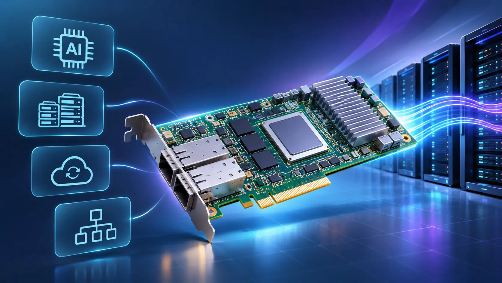
SuperNICs are specialized network accelerators designed for AI computing infrastructure. They are primarily used to enable high-speed, low-latency data communication between GPU servers. Through network processing acceleration and other technologies, they improve data transmission efficiency between servers and serve as one of the key hardware components enabling high-speed network interconnection in large-scale AI computing clusters. As an essential part of SuperNICs, SuperNIC PCBs support related chips and circuitry while providing the electrical connections and interconnections required for high-speed signal transmission.
Compared with conventional network interface cards, SuperNICs place greater emphasis on network transmission efficiency, remote direct memory access (RDMA), and congestion control in AI computing environments. NVIDIA's SuperNIC product family is one example of this development, reflecting the shift toward higher bandwidth and greater transmission efficiency in AI server networks. As network interface speeds increase, the associated high-speed PCBs face stricter requirements for material loss characteristics, impedance control, and multilayer interconnection quality.
To meet the evolving PCB manufacturing requirements of SuperNICs and AI server networking equipment, HoYoGo is a professional high-speed SuperNIC PCB manufacturer specializing in high-reliability, high-precision, multilayer, and high-speed PCB manufacturing. The company provides customized PCB manufacturing services to meet the technical requirements of different applications.
High-Speed Signal Transmission and Impedance Control
SuperNICs can connect to host servers or computing platforms through PCIe interfaces and communicate with other servers and networking equipment through high-speed network interfaces. Taking NVIDIA ConnectX-8 SuperNIC as an example, it is offered in two form factors: a PCIe adapter card and an OCP 3.0 card. The associated PCBs must support multiple high-speed differential signal pairs while meeting strict impedance control and signal integrity requirements. Precise circuit fabrication and tight impedance tolerance control are therefore important aspects of high-speed PCB manufacturing.
PCB trace impedance is influenced by factors such as trace width, differential pair spacing, finished copper thickness, dielectric thickness, and material dielectric constant (Dk). Trace width deviations caused by etching and changes in dielectric thickness during multilayer lamination can cause finished trace impedance to deviate from its target value. PCB manufacturers must control trace dimensions and dielectric thickness according to customer-specified stack-up structures, impedance targets, and technical specifications. Impedance testing is then performed as required to verify that the finished PCBs meet the specified impedance tolerances.
Low-Loss Materials and High-Speed Transmission Performance
The transmission performance of high-speed signal channels in SuperNICs is closely related to PCB material properties. Dielectric loss and conductor loss are major contributors to channel loss during high-speed data transmission. For high-speed network boards with longer transmission paths or stringent channel loss budgets, materials that meet the specified loss requirements can help reduce signal attenuation along PCB transmission lines.
During PCB manufacturing, material specifications must be followed, with attention to dielectric constant (Dk), dissipation factor (Df), and copper conductor surface roughness. For high-speed networking boards using low-loss PCBs, appropriate material selection and process control help minimize signal transmission losses and maintain consistent electrical performance. Df is closely associated with dielectric loss, while copper surface roughness affects conductor loss at high frequencies. High-speed PCB materials vary in lamination characteristics, dimensional stability, and processing requirements. Proper process control is essential to maintaining dimensional stability and consistent electrical performance throughout PCB fabrication. Manufacturers must control lamination quality and interlayer bonding reliability while ensuring that copper foil surface characteristics are compatible with the manufacturing processes used. These measures help minimize adverse effects on the transmission performance of finished PCBs.
Multilayer PCBs and High-Density Interconnections
SuperNIC boards typically integrate high-speed network controller chips, host interfaces, power management components, and other electronic devices. Some high-bandwidth products may require PCBs with higher layer counts to accommodate high-speed signal transmission, power distribution, and component interconnections. For boards with high interface density, layer-to-layer registration accuracy, drilling positional accuracy, and hole metallization quality are critical aspects of manufacturing process control.
Multilayer PCB manufacturing involves critical processes such as inner-layer circuit fabrication, lamination, drilling, and hole metallization. Layer-to-layer registration errors can affect the alignment of drilled holes with inner-layer pads, while the thickness, uniformity, and integrity of copper plating on hole walls influence interlayer connection reliability. For high-speed PCBs requiring backdrilling, manufacturers must control backdrill depth and via stub length according to customer technical specifications. This helps reduce the adverse effects of via stubs on high-speed signal transmission while avoiding damage to the functional connection layers.
Thermal Conditions and Long-Term Reliability
SuperNICs are typically deployed in AI servers and data center equipment that operate for extended periods. Heat generated by high-speed network chips and power management components may raise temperatures in localized areas of the PCB. Changes in equipment workload or repeated startup and shutdown cycles can cause temperature fluctuations. Combined with differences in thermal expansion among PCB materials, these changes may generate thermomechanical stress that affects the long-term reliability of interlayer bonding and plated-through-hole connections.
For data center operating environments, PCB manufacturers must consider substrate glass transition temperature (Tg), coefficient of thermal expansion (CTE), and heat resistance according to customer-specified operating temperature ranges and reliability requirements. Lamination and hole metallization quality must also be controlled. Where required, applicable thermal stress or temperature cycling tests should be performed according to customer technical specifications to assess PCB structural integrity and interconnection reliability under specified test conditions.
Volume Manufacturing and Quality Consistency
High-speed PCBs used in SuperNICs typically have stringent requirements for trace dimensions, impedance tolerances, and multilayer interconnection quality. During volume production, manufacturers must not only ensure compliance with technical specifications but also control variations between production batches. Consistency in trace dimensions, dielectric thickness, and hole metallization quality is essential to meeting subsequent assembly and board-level electrical performance requirements.
PCB manufacturers must maintain effective raw material batch management and control of critical manufacturing processes. Dimensional inspection, electrical testing, and impedance testing where required should be performed according to customer technical specifications. By maintaining production parameter records, analyzing inspection data, investigating quality issues, and tracing their causes, manufacturers can identify and address process deviations in a timely manner, reducing quality variations between production batches.
Development Trends in High-Speed PCBs for SuperNICs
As AI computing clusters expand, SuperNICs are evolving toward higher network bandwidth. Continued advances in high-speed networking technology place greater demands on PCB material loss characteristics, precision fabrication capabilities, and multilayer interconnection quality. For high-speed network boards with different interface specifications and transmission rates, PCB manufacturers must not only meet existing manufacturing tolerances but also adapt to changes in material systems and interconnection structures introduced by next-generation products.
SuperNIC products vary in interface specifications, board structures, and material requirements, resulting in different levels of PCB manufacturing complexity. Looking ahead, consistent processing of high-speed materials, precision circuit fabrication, and volume manufacturing capabilities for complex multilayer PCBs will be essential for meeting the requirements of next-generation high-speed networking equipment.
As a professional high-speed SuperNIC PCB manufacturer, HoYoGo has capabilities in precision circuit fabrication, low-loss material processing, and multilayer PCB manufacturing. The company provides customized PCB manufacturing services based on customer-specified material requirements, stack-up structures, and technical specifications. Through strict control of trace fabrication accuracy, impedance tolerances, and interlayer interconnection quality, HoYoGo helps ensure that finished SuperNIC PCBs meet the requirements for high-speed signal transmission and long-term reliability. Production and quality management are carried out in accordance with applicable IPC standards and customer specifications, supporting the PCB manufacturing needs of next-generation high-speed networking equipment and AI computing infrastructure.


 English
 Français
 Deutsch
 Português
 Pусский
 中文
