Welcome to visit Hoyogo website, let's connect the world together!
Customer service hotline:+86 13723413985 or 400 058 2288
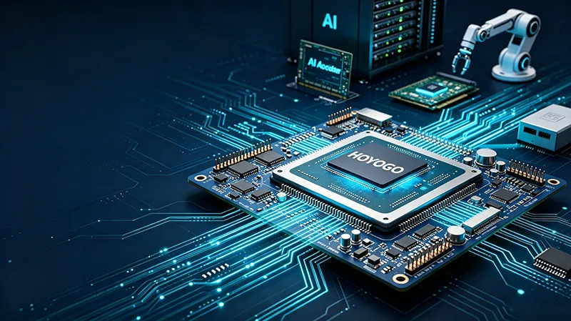
The rapid development of generative AI is accelerating the evolution of AI servers, AI accelerator cards, edge computing devices, AI PCs, intelligent robots, and other AI-powered hardware. As computing performance continues to increase, these systems must process and transmit growing volumes of data while operating at higher power and component densities. These changes are placing greater demands on PCB performance and manufacturing capabilities.
In high-performance AI computing systems, PCBs support key components such as GPUs, CPUs, AI accelerator chips, memory, and high-speed interfaces, while providing the foundation for high-speed signal transmission and power distribution. As data rates, component density, and power density increase, these trends are driving demand for high-speed, high-density, and high-reliability PCBs, placing stricter requirements on material processing, manufacturing precision, impedance control, layer-to-layer registration, and production consistency.
As a high-reliability PCB manufacturer, HoYoGo specializes in high-precision, high-density, multilayer, and high-speed PCB manufacturing for AI servers, AI computing systems, and a wide range of intelligent hardware.
High-Speed PCB Manufacturing Requires Greater Precision
AI computing systems require large amounts of data to be exchanged among processors, GPUs, memory, storage devices, and network interfaces. With the adoption of high-speed interfaces such as PCIe 5.0, DDR5, and high-speed SerDes, signal loss, impedance consistency, and signal integrity have become more sensitive to PCB manufacturing precision. Meanwhile, the development of 400G and 800G networking equipment is further increasing demand for high-speed PCBs.
For AI server PCBs and other high-speed computing PCBs, factors such as actual trace width, dielectric thickness, copper thickness, etching uniformity, and layer-to-layer registration can affect impedance and signal transmission performance. PCB manufacturers therefore need tighter process control over key manufacturing steps such as circuit fabrication, lamination, and impedance control to reduce the impact of manufacturing variations on final electrical performance.
High-Density Integration Drives the Use of Multilayer and HDI PCBs
AI hardware needs to integrate computing, storage, power, and high-speed communication functions within limited board space. As chip I/O counts and component density increase, PCB routing and interconnect structures become more complex, leading to wider use of multilayer PCBs and HDI PCBs in AI accelerator cards, high-performance computing modules, and other high-density electronic products.
HDI PCB manufacturing typically involves fine-line fabrication, laser drilling, microvia processing, and layer-to-layer registration. More complex HDI structures may also require multiple lamination cycles. Microvia quality, copper plating quality, and layer-to-layer registration accuracy can all affect the reliability of interlayer connections. PCB manufacturers therefore need tight control over key processes such as microvia fabrication, lamination, and plating to maintain the manufacturing quality and consistency of complex interconnect structures.
Higher Power Density Raises PCB Reliability Requirements
Higher AI chip performance is often accompanied by increased power consumption and power density. AI servers, AI accelerator cards, and high-performance computing equipment often operate under high loads for extended periods. This increases PCB current-carrying requirements and places greater demands on reliability under sustained thermal loads and temperature changes.
In high-power applications, factors such as copper thickness and uniformity, through-hole copper plating quality, interlayer bonding, and material heat resistance can affect long-term PCB reliability. PCB manufacturers therefore need to control copper thickness and key processes such as electroplating and lamination according to product requirements and material characteristics, reducing the impact of prolonged high-load operation and thermal cycling on PCB reliability.
Low-Loss Materials Raise PCB Manufacturing Requirements
As signal transmission speeds increase, PCB material properties such as dielectric performance and transmission loss have a greater impact on high-speed signals. Low-loss high-speed laminates are increasingly used in AI servers, high-speed network switches, and high-performance computing platforms to support high-speed data transmission.
Different high-speed materials have different processing characteristics during lamination, drilling, and circuit fabrication, placing greater demands on the control of dielectric thickness, circuit accuracy, and impedance consistency. PCB manufacturers need to adjust relevant process parameters according to material characteristics to maintain stable and consistent high-speed PCB manufacturing.
High Reliability Requires Control Throughout PCB Manufacturing
AI servers and data center equipment typically operate continuously for extended periods, placing greater demands on PCB reliability and production consistency. Factors such as through-hole copper plating quality, interlayer connections, material heat resistance, and circuit fabrication quality can all affect PCB stability during long-term operation.
From raw material management and inner-layer circuit fabrication to lamination, drilling, copper deposition, electroplating, surface finishing, and final inspection, stable process control is required throughout PCB manufacturing. Electrical testing, impedance testing, microsection analysis, and necessary reliability testing can be used to evaluate key PCB quality parameters, reduce the risk of potential manufacturing defects, and improve consistency in volume production.
AI Hardware Is Driving Advances in PCB Manufacturing
AI applications are expanding from data centers into industrial equipment, intelligent robots, automotive electronics, edge computing, and a wide range of intelligent devices. Different applications have different requirements for data transmission speed, integration density, power, and operating environments, resulting in different PCB manufacturing requirements.
As AI hardware continues to evolve, PCB manufacturers need to advance their capabilities in high-speed material processing, precision circuit fabrication, high-density interconnects, process control, and quality verification to meet increasingly complex PCB manufacturing requirements.
As a professional PCB manufacturer, HoYoGo specializes in high-precision, multilayer, HDI, and high-speed PCB manufacturing. We provide production services based on the PCB specifications and manufacturing requirements of AI servers, AI computing systems, intelligent robots, and other high-performance electronic products, with strict process control and quality inspection to maintain manufacturing quality and consistency across production batches.


 English
 Français
 Deutsch
 Português
 Pусский
 中文
中文