Welcome to visit Hoyogo website, let's connect the world together!
Customer service hotline:+86 13723413985 or 400 058 2288
The rapid growth of AI data centers, high-performance computing, and cloud networking is driving demand for greater data transmission capacity within data centers. Optical communication equipment is evolving toward higher transmission rates and greater port density. With 400G and 800G optical communication technologies becoming more widely adopted, 1.6T optical transceivers and high-speed switching equipment represent an important next stage of development. Increasing transmission rates place greater demands not only on optical transceiver performance but also on PCB signal integrity, interconnection density, and long-term reliability.
PCBs provide the electrical connections and high-speed signal paths between components in optical communication equipment, including optical transceivers, data center switches, and associated control units. For high-speed PCBs used in 1.6T applications, material loss characteristics, impedance control accuracy, circuit fabrication precision, multilayer interconnection quality, and manufacturing consistency can all influence the performance of the finished product.
HoYoGo is a professional 1.6T Optical Communication PCB manufacturer specializing in high-speed, high-reliability, high-precision and multilayer PCB manufacturing. To meet the requirements of 1.6T optical communication equipment, PCB manufacturing must focus on low-loss materials, high-speed signal transmission and impedance control, high-density interconnection processes, and long-term operational reliability.
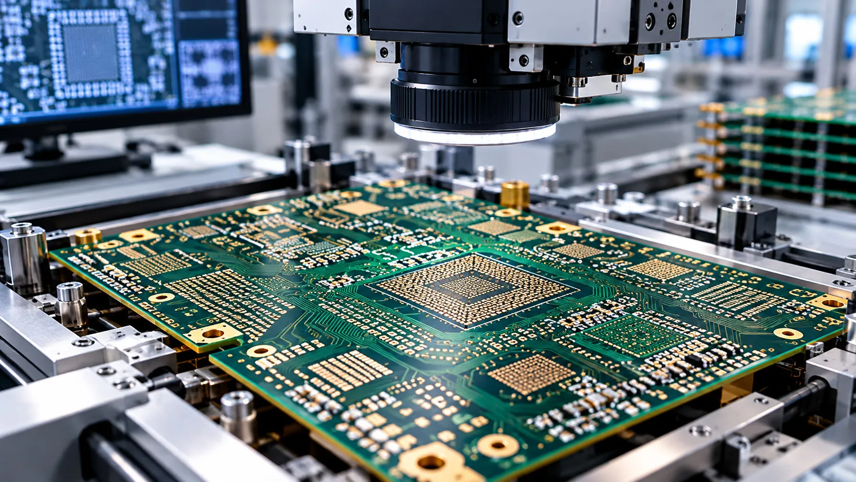
High-Speed Signal Transmission and Impedance Control
1.6T optical communication equipment typically employs multichannel high-speed data transmission architectures. Some 1.6T optical transceivers employ eight electrical lanes operating at approximately 200 Gb/s per lane, using 224G-class PAM4 signaling technology. In such high-speed interconnect applications, PCB traces must exhibit low transmission loss and meet stringent impedance control requirements.
The actual impedance of controlled-impedance traces depends on factors such as trace width, copper thickness, dielectric thickness, and dielectric constant (Dk). Differential pairs also require precise control of trace spacing and manufacturing tolerances. During production, etching accuracy, copper thickness, and dielectric thickness must be controlled according to customer-specified stack-up structures, impedance targets, and technical specifications. Impedance testing is used to verify that the manufactured traces fall within the specified impedance tolerance range.
For some high-speed PCBs using plated through-hole interconnections, via stubs can cause signal reflections and affect signal integrity. Back drilling may be applied according to customer design requirements to reduce stub length. Manufacturing control must account for the PCB stack-up and target layer positions to maintain the required back-drill depth, positional accuracy, and remaining stub length.
Low-Loss Materials and Manufacturing Stability
In high-speed optical communication equipment, the electrical properties of PCB materials directly affect signal transmission performance. Dielectric constant (Dk) influences signal propagation characteristics, while dissipation factor (Df) affects dielectric loss during signal transmission. Copper foil surface roughness also contributes to conductor loss at high frequencies.
Material selection for 1.6T high-speed applications depends on operating frequency, transmission distance, and specific product requirements. In addition to meeting electrical performance specifications, the selected materials must offer suitable dimensional stability, thermal properties, and processing characteristics.
During manufacturing, critical processes such as lamination, drilling, and circuit fabrication must be controlled according to material properties and product specifications. Consistent dielectric thickness, accurate layer-to-layer registration, and stable processing conditions help minimize the effects of manufacturing variations on high-speed signal performance and maintain quality across production batches.
High-Density Circuits and Multilayer Interconnections
As optical communication equipment incorporates more ports and increasingly integrated hardware, PCBs must accommodate high-speed signals, power connections, and control circuits within limited board space. This places greater demands on fine-line fabrication, layer-to-layer registration, and hole processing accuracy.
Multilayer PCB manufacturing involves critical processes such as inner-layer circuit fabrication, lamination, drilling, and hole metallization. Accurate layer-to-layer registration, precise hole positioning, and consistent plated hole quality are essential to interconnection reliability.
Some high-density optical communication PCBs may use HDI structures, including any-layer HDI configurations, as well as via-in-pad technology, depending on component placement and signal integrity requirements. Manufacturing these boards requires precise control of circuit dimensions and microvia quality, along with reliable interlayer connections.
Thermal Conditions and Long-Term Reliability
Some 1.6T optical transceivers and high-speed switching equipment operate at relatively high power densities. Heat generated during continuous operation may expose PCBs to elevated temperatures, while changes in operating conditions can subject them to thermal cycling.
PCB material selection and manufacturing processes must account for the intended operating environment and customer specifications. Important considerations include glass transition temperature (Tg), coefficient of thermal expansion (CTE), and interlayer bonding properties. Maintaining lamination quality, uniform copper plating in through-holes, and material compatibility helps reduce the risk of delamination, cracking, and other reliability issues during long-term operation.
Volume Production and Quality Consistency
For high-speed PCBs used in 1.6T optical communication equipment, variations in trace dimensions, dielectric thickness, copper thickness, and hole processing quality can affect impedance stability, dimensional accuracy, and interconnection reliability.
Consistent production quality depends on effective raw material management and control of critical manufacturing processes. Statistical process control (SPC) helps monitor manufacturing variations, while impedance testing, electrical testing, and applicable reliability verification help confirm that PCBs from different production batches meet the specified requirements.
1.6T Optical Communication PCB Manufacturing and Quality Control
The development of 1.6T optical transceivers and high-speed optical communication equipment is placing greater demands on PCB manufacturing capabilities and quality control. Signal rates, board structures, and operating environments vary across products, making it necessary to adapt material selection, circuit fabrication, interconnection processes, and reliability controls to specific technical requirements.
As a professional 1.6T Optical Communication PCB manufacturer, HoYoGo specializes in high-speed and high-reliability PCB manufacturing. We provide customized PCB manufacturing services for high-speed optical transceivers, data center switching equipment, and related optical communication products, covering low-loss material processing, impedance control, HDI manufacturing, and reliability testing. By following applicable IPC standards and customer technical specifications, we maintain control over critical manufacturing processes and product quality to provide reliable PCB manufacturing support for high-speed optical communication equipment.


 English
 Français
 Deutsch
 Português
 Pусский
 中文
中文