Welcome to visit Hoyogo website, let's connect the world together!
Customer service hotline:+86 13723413985 or 400 058 2288
As industrial robotics, smart manufacturing, and automated logistics technologies continue to advance, 3D vision systems are increasingly being used in robotic picking, workpiece positioning, automated assembly, and spatial perception. Compared with conventional 2D vision, 3D vision systems can capture depth information and three-dimensional spatial features, providing the data robots need to determine target positions, identify object poses, and perform precision operations. These applications are driving demand for robotic 3D vision PCBs that support reliable data acquisition, signal transmission, and integration of vision-related electronic modules.
Common imaging technologies used in robotic 3D vision systems include stereo vision, structured light, time-of-flight (ToF), and laser triangulation. These technologies differ in their imaging principles, data acquisition methods, and hardware configurations. For example, ToF technology determines depth by measuring the time taken for light signals to travel to and return from an object, while laser triangulation calculates distance by analyzing changes in the position of projected laser points. The associated equipment typically incorporates image or depth sensors, data processing components, communication interfaces, and power management modules. PCBs serve as essential platforms for component mounting, electrical interconnection, signal transmission, and power distribution within electronic modules. Differences in module integration and interface configurations also result in varying requirements for PCB fabrication accuracy, interlayer connections, and electrical performance.
HoYoGo is a professional robotic 3D vision PCB manufacturer specializing in high-reliability, high-precision, multilayer, and high-speed PCB manufacturing. To meet the requirements of visual data acquisition, signal transmission, and electronic module integration, the company focuses on circuit fabrication accuracy, interlayer connection quality, and consistency in volume manufacturing. Impedance control is also implemented according to product specifications, enabling HoYoGo to provide customized PCB manufacturing services for robotic 3D vision equipment.
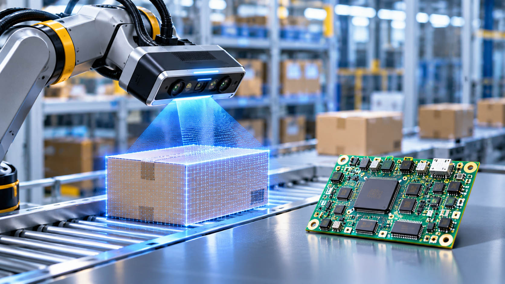
3D Vision Data Acquisition and High-Speed Signal Transmission
Robotic 3D vision systems must capture image or depth information and transmit the data to processing units. Stereo vision systems use two imaging units to capture images from different viewpoints, while structured light systems project specific light patterns onto target objects and capture the resulting pattern variations to calculate surface depth information. Equipment using high-resolution imaging, high frame rates, or multiple sensors typically generates larger volumes of data, placing greater demands on PCB signal transmission quality through high-speed digital interfaces. For 3D vision system PCBs, maintaining signal integrity through appropriate stack-up design, controlled impedance, and precise circuit fabrication is important for supporting reliable data transmission.
During PCB manufacturing, factors such as trace width, finished copper thickness, dielectric thickness, and material dielectric constant (Dk) influence trace impedance and signal propagation characteristics. Differential pair spacing is another important factor affecting differential impedance. In addition, material dissipation factor (Df) and conductor surface roughness influence high-speed signal transmission loss. For PCBs requiring controlled impedance, manufacturers must control trace dimensions and relevant fabrication parameters according to customer-specified stack-up structures, impedance targets, and technical specifications. Impedance testing and any necessary electrical performance tests must also be performed as required.
High-Density Vision Modules and Multilayer Interconnections
Some robotic 3D vision modules must integrate image sensors, processors, memory, and communication interfaces within limited space. Structured light and active ToF modules also incorporate light-source driving and control circuits. As vision modules become smaller and more highly integrated, certain products place greater demands on fine-line PCB fabrication, pad size and positional accuracy, and multilayer interconnection quality. These requirements make high-precision PCB manufacturing particularly important for compact and highly integrated robotic vision modules.
Manufacturing these PCBs involves circuit fabrication, layer-to-layer registration, lamination, drilling, and hole metallization. Pad dimensions and positional accuracy affect compatibility with component assembly, while drilling accuracy and layer registration influence the alignment of holes with inner-layer pads. The thickness, uniformity, and integrity of plated copper on hole walls directly affect the reliability of interlayer electrical connections. For multilayer PCBs incorporating high-density interconnect (HDI) structures, particular attention must also be given to microvia fabrication, metallized interconnections, and lamination quality to ensure that interlayer connections meet product requirements.
Thermal Reliability of Vision Sensors and Processing Modules
Image sensors, processors, and power management components generate heat as robotic 3D vision systems continuously acquire and process data. In highly integrated vision modules, component power consumption, limited installation space, and heat dissipation conditions may lead to localized temperature increases on the PCB. Some systems using active illumination also contain light sources and driver circuits, whose power consumption can further affect local temperature distribution across the board.
Differences in the coefficients of thermal expansion (CTE) among PCB materials can generate thermomechanical stress during temperature changes. Prolonged thermal cycling may affect the reliability of interlayer bonding and plated interconnection structures. PCB manufacturers must consider substrate glass transition temperature (Tg), coefficient of thermal expansion (CTE), and other relevant properties according to the product's operating temperature range and reliability requirements. Particular attention should be paid to the compatibility between Z-axis thermal expansion characteristics and plated-through-hole copper structures. Controlling lamination and hole metallization quality helps reduce the risk of delamination, barrel cracking, and interconnection failures under thermal cycling conditions.
PCB Reliability in Robotic Operating Environments
Robotic 3D vision systems may be mounted on robotic arm end effectors, robot bodies, or fixed vision inspection stations, each with different operating conditions. Vision modules installed on moving mechanisms may be exposed to mechanical vibration and inertial loads caused by repeated acceleration and deceleration. Although fixed modules are not directly subjected to inertial loads from robot movement, they may still experience vibration from operating equipment or the surrounding environment. Humidity and dust must also be considered in certain industrial applications.
To address these operating conditions, PCB manufacturers must control substrate properties, interlayer connection quality, and critical manufacturing processes according to product specifications. Surface finish quality, board cleanliness, and insulation performance also require attention. For products with specific environmental requirements, additional protection measures and reliability verification should be considered in accordance with customer specifications. PCB manufacturing quality provides an important foundation for the long-term stable operation of vision modules, while overall vibration resistance and imaging stability also depend on mechanical mounting, optical structures, and component assembly.
Volume Manufacturing and Quality Consistency
Robotic 3D vision systems vary in imaging technology, communication interfaces, and module specifications, resulting in different PCB layer counts, circuit structures, and manufacturing processes. For products incorporating fine-line circuitry, high-density packaged components, and high-speed communication interfaces, volume manufacturing must not only meet the technical requirements of individual production batches but also maintain consistent trace dimensions, pad accuracy, and interlayer connection quality across batches.
During volume production, PCB manufacturers must maintain effective raw material management and tight control over critical processes, including circuit fabrication, lamination, drilling, and hole metallization. This helps reduce the impact of process variations on finished board quality. Visual inspection, dimensional inspection, and electrical testing should be conducted according to customer technical specifications, with impedance testing and applicable reliability verification performed where required. These measures help ensure that PCBs delivered in volume meet the specified quality requirements.
Development Trends in PCBs for Robotic 3D Vision Systems
As industrial robots are increasingly used for complex object recognition, precision picking, and automated assembly, 3D vision systems face growing demands for data acquisition speed, processing capability, and hardware integration. Multi-sensor operation, real-time image processing, and high-speed interfaces are driving some vision modules toward smaller form factors and higher levels of integration.
As integration levels continue to increase, PCB requirements will become more diverse in terms of layer count, interconnection structures, material selection, and manufacturing precision. PCB manufacturers must align their manufacturing processes and quality control requirements with the interface configurations, installation space, and operating environments of specific products. Precision circuit fabrication, multilayer interconnection manufacturing, material compatibility, and stable volume production will remain important priorities in PCB manufacturing for robotic 3D vision systems.
HoYoGo is a professional robotic 3D vision PCB manufacturer specializing in high-reliability, high-precision, multilayer, and high-speed PCB manufacturing. The company develops PCB manufacturing processes based on customer-specified product structures, material requirements, and reliability standards. Production and quality control are carried out in accordance with applicable IPC standards and customer technical specifications. HoYoGo provides reliable PCB manufacturing support for industrial robots, machine vision systems, and intelligent automation equipment, including customized machine vision PCBs for different application requirements.


 English
 Français
 Deutsch
 Português
 Pусский
 中文
